
Figure 4.10 (a) Circuit symbol for the n-channel enhancement-type MOSFET. (b) Modified circuit symbol with an arrowhead on the source terminal to distinguish it from the drain and to indicate device polarity (i.e., n channel). (c) Simplified circuit - PowerPoint PPT Presentation
Title:
Figure 4.10 (a) Circuit symbol for the n-channel enhancement-type MOSFET. (b) Modified circuit symbol with an arrowhead on the source terminal to distinguish it from the drain and to indicate device polarity (i.e., n channel). (c) Simplified circuit
Description:
Figure 4.10 (a) Circuit symbol for the n-channel enhancement-type MOSFET. (b) Modified circuit symbol with an arrowhead on the source terminal to distinguish it from ... – PowerPoint PPT presentation
Number of Views:336
Avg rating:3.0/5.0
Title: Figure 4.10 (a) Circuit symbol for the n-channel enhancement-type MOSFET. (b) Modified circuit symbol with an arrowhead on the source terminal to distinguish it from the drain and to indicate device polarity (i.e., n channel). (c) Simplified circuit
1
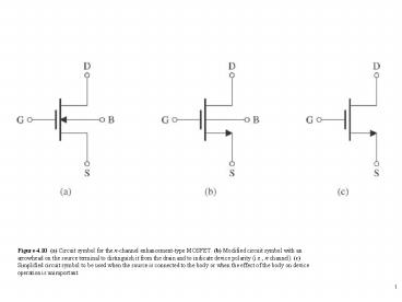
Figure 4.10 (a) Circuit symbol for the n-channel
enhancement-type MOSFET. (b) Modified circuit
symbol with an arrowhead on the source terminal
to distinguish it from the drain and to indicate
device polarity (i.e., n channel). (c)
Simplified circuit symbol to be used when the
source is connected to the body or when the
effect of the body on device operation is
unimportant.
2
Figure 4.11 (a) An n-channel enhancement-type
MOSFET with vGS and vDS applied and with the
normal directions of current flow indicated. (b)
The iDvDS characteristics for a device with kn
(W/L) 1.0 mA/V2.
3
Figure 4.12 The iDvGS characteristic for an
enhancement-type NMOS transistor in saturation
(Vt 1 V, kn W/L 1.0 mA/V2).
4
Figure 4.13 Large-signal equivalent-circuit
model of an n-channel MOSFET operating in the
saturation region.
5
Figure 4.14 The relative levels of the terminal
voltages of the enhancement NMOS transistor for
operation in the triode region and in the
saturation region.
6
Figure 4.15 Increasing vDS beyond vDSsat causes
the channel pinch-off point to move slightly away
from the drain, thus reducing the effective
channel length (by DL).
7
Figure 4.16 Effect of vDS on iD in the
saturation region. The MOSFET parameter VA
depends on the process technology and, for a
given process, is proportional to the channel
length L.
8
Figure 4.17 Large-signal equivalent circuit
model of the n-channel MOSFET in saturation,
incorporating the output resistance ro. The
output resistance models the linear dependence of
iD on vDS and is given by Eq. (4.22).
9
Figure 4.18 (a) Circuit symbol for the p-channel
enhancement-type MOSFET. (b) Modified symbol with
an arrowhead on the source lead. (c) Simplified
circuit symbol for the case where the source is
connected to the body. (d) The MOSFET with
voltages applied and the directions of current
flow indicated. Note that vGS and vDS are
negative and iD flows out of the drain terminal.
10
Figure 4.19 The relative levels of the terminal
voltages of the enhancement-type PMOS transistor
for operation in the triode region and in the
saturation region.
Recommended
CrystalGraphics Presentations


