Silicon Detector EM Calorimetry - PowerPoint PPT Presentation
1 / 18
Title:
Silicon Detector EM Calorimetry
Description:
Title: This Detec Author: Martin Breidenbach Last modified by: Martin Breidenbach Created Date: 5/24/2001 8:01:57 PM Document presentation format – PowerPoint PPT presentation
Number of Views:119
Avg rating:3.0/5.0
Title: Silicon Detector EM Calorimetry
1
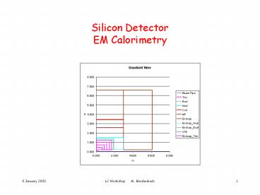
Silicon DetectorEM Calorimetry
2
SD (Silicon Detector)
- Conceived as a high performance detector for NLC
- Reasonably uncompromised performance
- But
- Constrained Rational cost
- We accept the notion that excellent energy flow
calorimetry is required, and explore optimization
of a Tungsten-Silicon EMCal
3
Silicon Tungsten EMCal
- Figure of merit something like BR2/s, where s is
the rms sum of Moliere radius of the calorimeter
and the pixel size. - Maintain the great Moliere radius of tungsten (9
mm) by minimizing the gaps between 2.5 mm
tungsten plates. Dilution is (1Rgap/Rw) - Could a layer of silicon/support/readout etc fit
in a 2.5 mm gap? Even less?? 1.5 mm goal?? - Requires clever electronic-mechanical integration!
4
EMCal, continued
- Diode pixels between 5 10 mm square on largest
hexagon fitting in largest available wafer. (6
available now 300 mm when??) Consider m
tracking as well as E flow in picking pixel
dimension. - Develop readout electronics of preamplification
through digitization, zero suppression and IO on
bump bonded chip. Upgrade would be full
integration of readout on detector wafer. (RD
opportunity!) - Optimize shaping time for small diode
capacitance. Probably too long for significant
bunch localization within train. But some
detector element needs good time resolution!!!
5
Channel Counts Forget Them!!
- We are used to pixel counts in CCDs
- 3x10⁸ last time, 1x10⁹ this time, no problem
- Silicon Strip Tracker 5x10⁶ strips (channels??)
- EMCal 5x107 pixels (channels??)
- Dont even think about multiplying channels by
O(10) - Must solve the cluster technology challenges.
6
Structure
7
Gross System Architecture
Silicon Diode Array
Readout Chip
Network Interconnect
8
Pixels on 6 Wafer
9
Zoom to Readout Chip
10
Cross Section
11
Signal Collection from m2 board
12
Preamplifier Architecture
- Charge amplifier and shaper followed by three
amplifiers with gains G1,G2,G3 and sample
holds. - Comparator logic to select appropriate range
- Mux and 12 bit ADC
13
Noise and Muons
- Assume 300 m (400-500 m possible) effective e-
collection at 80 e-/m. s0.6. So S/N5 seems
rational goal. - 1 SD noise would be 4800 e-. Assuming diode
capacitance of 1 pf/mm2, and amplifier noise of
20e-/pf200 get about factor of two safety! (1
MIP 2 x 10⁴ e-)
14
Plausible Resolution Criteria
- Spread the 0.6 muon s into several bins, with
enough range for MIP counting to a few. - Preliminary Monte Carlo indicates peak ionizing
track density from a high energy shower to be
2200 µ equivalent. (5 x 10⁷ e- 8 pC.) - Do not degrade resolution of calorimeter! Energy
resolution of a sampling calorimeter with 2/3 X0
plates will not exceed 12/vE. Say this peak
should be spread over 5 bins, and take no credit
for multiple sampling.
15
Low end resolution requirements
- Res 1 Bin Width50e-, Emax1.9 Gev, Mips8.5
16
Required Resolution
- Res 2 Bin Width1300 e-, Emax50 GeV,Mips225
- Res 3 Bin Width13000 e-,Emax512 GeV,Mips2325
17
Technical Issues
- Assuming integrator full scale voltage of around
1 V, feedback (and calibration) capacitors need
to be 10 pF. This is large for an integrated
capacitor, but doable with substantial real
estate. - Plus is that this makes the bump bond pitch easy!
- Cooling GLAST system is 2 mW/channel. Assume
1000 pixels/wafer and power pulsing duty factor
for NLC of 10-3 (10 µsec _at_120 Hz). HD18 (95W,
3.5 Ni, 1.5 Cu) is possible alloy. s18gm/cm3,
sc0.33 w/cm-0C. Assume cooling on one edge,
then ?T2.50C. This is fine, but it sure doesnt
work without power pulsing!!! Need to consider
possibility of copper layer in the G10.
18
Plans
- We (Oregon and SLAC) plan to develop this design
in more detail and (hopefully) build prototype
wafers and chips. - If successful, develop board level chip.
- Build 1 wafer wide by about 25 X0 deep
calorimeter for test beam.


