
Ultra High Speed InP Heterojunction Bipolar Transistors - PowerPoint PPT Presentation
Title:
Ultra High Speed InP Heterojunction Bipolar Transistors
Description:
Mattias Dahlstr m Trouble is my business, (Raymond Chandler) Ultra High Speed InP Heterojunction Bipolar Transistors Introduction to HBT s How to make a fast HBT – PowerPoint PPT presentation
Number of Views:343
Avg rating:3.0/5.0
Title: Ultra High Speed InP Heterojunction Bipolar Transistors
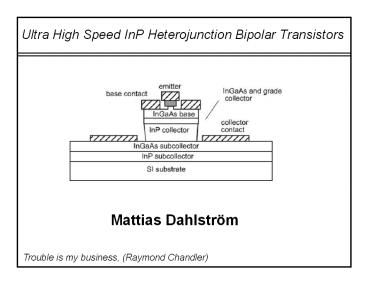
1
Ultra High Speed InP Heterojunction Bipolar
Transistors
- Mattias Dahlström
Trouble is my business, (Raymond Chandler)
2
Ultra High Speed InP Heterojunction Bipolar
Transistors
- Introduction to HBTs
- How to make a fast HBT
- Delay terms
- The graded base
- The base-collector grade
- Recent results
- Record fmax mesa DHBT
- Record f? DHBT
- details regarding this to follow
3
The transistor
Small change in base current ? large change in
collector current
Schematic of an HBT
Typical common-emittercharacteristics
4
InP lattice structure
Nearest neighbor 2.5 A Lattice constant 5.86 A
5
InP
InGaAs
InP and InGaAs have G-L separations of 0.65
eV, vs 0.4 eV for GaAs? larger collector
velocityInGaAs has a low electron effective mass
? lower base transit time
6
Objectives and approach
Objectivesfast HBTs ? mm-wave power, 160 Gb
fiber opticsdesired 440 GHz ft fmax, 10
mA/mm2, Ccb/Iclt0.5 ps/Vbetter manufacturability
than transferred-substrate HBTsimproved
performance over transferred-substrate
HBTs Approach narrow base mesa ? moderately
low Ccb very low base contact resistance
required, and good alignment ? carbon base
doping, good base contact process high ft
through high current density, thin layers bandgap
engineering small device transit time with
wide bandgap emitter and collector
7
Potential uses of InP HBT
- Communication systems
- wireless communication, fiber optics
transceivers, - digital processing in radar (ADCs, DACs)
- Types of circuits
- broadband amplifiers, power amplifiers,
laser/modulator drivers - comparators, latches, fast logic
- Circuit characteristics
- 1-10 000 HBTs per IC
- Very high demands for speed (40-200 GHz)
- Fast logic with moderate power consumption (20
mW/gate) - Moderate Output Power mmwave power amps,
optical modulator drivers 6 V at Jc4 mA/µm2 ,
2 V at Jc8 mA/µm2
8
DHBT band diagram under bias
emitter
collector
base
9
High speed HBT some standard figures of merit
- Small signal current gain cut-off frequency
(from H21) - Maximum power gain ( from U)
- Collector capacitance charging time when
switching
10
Scaling laws for fast HBTs
for x 2 improvement of all parasitics ft, fmax,
logic speedbase Ö2 1 thinnercollector 21
thinneremitter, collector junctions 41
narrowercurrent density 41 higheremitter Ohmic
41 less resistive
transferred-substrate
Challenges with ScalingCollector mesa HBT
collector under base Ohmics. Base Ohmics must be
one transfer lengthsets minimum size for
collector Emitter Ohmic hard to improvehow
?Current Density dissipation, reliabilityLoss
of breakdownavalanche Vbr never less than
collector Eg (1.12 V for Si, 1.4 V for InP)
.sufficient for logic, insufficient for power
narrow collector mesa
11
Contact resistance tunneling through barrier
Theory idealized contact
- High doping 1-9 1019 cm-3
- Small bandgap InAsltInGaAsltInPltGaN
- Surface preparation no interstitial oxide
- Metal reactions
12
Pd-based contacts
Ohmic contact to p-type material 10-100 times
worse than n-type. Work function line-up,
electron/hole effective mass
- Pd/Pt reacts with III-V semiconductor
- InGaAsPd ? As (In,Ga)Pd(In,Ga)(Pd,As)
- Pd reaction depth 4 x thickness
- 25 Å Pd for 300 Å base
- Contact resistance
- 100-500 ?-?m2 ?1-20 ?-?m2
- from TLM and RF-extraction
Yu, J.S. Kim, S.H. Kim, T.I. PtTiPtAu and
PdTiPtAu ohmic contacts to p-InGaAs,
Proceedings of the IEEE Twenty-Fourth
International Symposium on Compound
Semiconductors, San Diego, CA, USA, 8-11 Sept.
1997
13
Emitter resistance
14
Emitter resistance grades removed
InGaAs cap layer
InP emitter
light doping
Contact resistance 50 ??m2 ? 25 ??m2 ? 15
??m2 High doping ? 3 1019 cm-3 No InGaAs-InP
grade necessary at very high doping Thin
undepleted n- emitter Small emitter area
increases Rex
heavy doping
At degenerate doping levels grades are not
necessary
15
Base resistance
TLM measurement
Rbb is a critical parameter for fmax, and in npn
HBT the base contact resistance dominates. Rbb
is minimized through high base doping and
improved base contact metallization, small
undercut Wgap, and long emitter Le
16
Problems with very thin bases
- Etching and depletion effects reduce the
effective base thickness Tb, and increases the
base resistance. - At 500 nm scaling generation, best base thickness
is 30-40 nmbetter fmax , lower Rbb-related
delay terms in gate delay ,minimal improvement
in ft between 25 30 nm
High resistance
17
Increase of sheet resistance with thin base layers
Rb,extrinsic800-1000 O/sq Rb,intrinsic600-750
O/sq
Base surface exposed
InGaAs base doped 6 1019 cm-3, surface pinned at
0.18 eV. Surface depletion decreases base
thickness 40 Å.
Base protected by E/B grade (contacts diffused
through 160 Å grade)
Surface depletion Wet etching
18
Collector resistance
Rc access resistance between collector contact
and the mesa. Minimized by large collector
contacts, and low resistance subcollector
19
Subcollector design
- Goals
- minimize electrical resistance
- minimize thermal resistance
- limit thickness to improve manufacturability
- Thermal conductivity of InGaAs 5 W/mK
- Thermal conductivity of InP 68 W/mK
Etch stop layer provides collector undercut
less Cbc
Some still use all InGaAs subcollector Subcollect
or resistivity 500 A InGaAs 2000 A InP 11
?/sq 125 A InGaAs 3000 A InP 9 ?/sq
- 53 of thermal resistance
Etching selectivity of InGaAs vs. InP main limit
? 50 A InGaAs Contact resistance better to 125 A
than 50 A after annealing
20
Base-emitter capacitance
Cje is the junction capacitance between the
emitter and base Cje corresponds to 100 Å
depletion thickness Minimized by shrinking the
emitter area at fixed or at increasing current
Ic
21
Base-collector capacitance
Cbc is the junction capacitance between the base
and subcollector.
22
Base-collector capacitance
Breakdown limits thickness
Collector thickness reduced due to speed
requirements
Thickness (A) Breakdown (V)
2150 7.5
1500 4-5
Ccb increases !
- Tc 3000 A ? 2150 A ? 1500 A
- Abc must be kept small
- narrow emitter
- narrow base contacts
- undercut of base contacts
- implant or regrowth
23
Theory of the base
- If gain is limited by Auger recombination in the
base
The base sheet resistance
The base transit time
- Decreasing increases .
- High Na and Tb for low ?s decreases
- Grade gives 30-50 improvement
ps is 400-900 ?/sq
is 100-250 fs
24
Base Transit Time
Fitting of relevant parameters of the form
Kroemers double integral Drift-Diffusion
equation for base current
With doping as
Intrinsic carrier concentration
Exit term
Diffusivity
Ballistic injection
Solution used for evaluation of the base transit
time
25
Base grading
Graded bandgap
Graded doping
Change in InGa ratio InAs Eg0.36 eV GaAs
Eg1.43 eV
Doping 8 ? 5 1019 cm-3
26
Base grading induced electric field
Limits Bandgap narrowing, needs degenerate
doping
Limits strain
Induced electric field accelerates electrons
towards collector decreases base transit time
and increases gain
27
The effect of degenerate doping
Strong variation in Fermi-level with doping at
high doping levels
Evidence Observed Vbe increase Von fbi ,
increases with Ev Nb4 1019cm3?0.75 V Nb8
1019cm3?0.83 V for graded base-emitter
28
Base bandgap narrowing
Bandgap grade
Doping grade
Model after V. Pavlanovski
BGN provides an electric field opposing the
doping-induced field. 15 in magnitude
29
Base Transit time
Ballistic effects may arise when Tblt180-200 _at_5
1019 cm-3 (Tessier, Ito)
Bandgap grade and doping grade give same ?b
Results Bandgap graded Doping graded DC
gain 25 18 ft 250 GHz 282 GHz
30
Collector design
Transit time Close inspection show velocity
near base most important
- Use grade
- Use setback
31
Base-collector grade
- Early grade designs
- Too coarse
- No setback layer
Gain 7 f? 128 GHz (Tc3000 A) Jkirk 1.3 mA/µm2
- Recent grade designs
- 15 A period
- 200 A setback layer
Gain 27 f? 282 GHz (Tc2150 A) Jkirk 4 mA/µm2
32
InAlAs/InGaAs super lattice
- Why super lattice?
- MBE is more suited for super lattice than
quaternaries. - InP/InGaAs gives poor quality material due to
phosphorous-arsenic intermixing - MOCVD growth ? InGaAsP grade
- GaAsSb base needs no grade
33
Quantum mechanical trapping in grade
- Quantum well trapping
- Electron/hole in the InGaAs well
- 500 meV InAlAs potential barrier
- A rough approximation the infinite potential
well.
If Engt 500 meV (InGaAs/InAlAs potential) ? no
electron confinement 31 A is the maximum
allowed InGaAs width by this model
34
The delta-doping
H. Kroemer a conduction band difference can be
offset with a grade and a delta-doping
No delta-doping
Delta-doping
Vbc0.3 V
Vbc0.3 V
With this choice the conduction band will be
smooth
35
The setback layer
- An InGaAs layer beneath the base
- Margin for Base dopant diffusion
- Increases Electron speed at SL
Setback
No setback
Vbc0.3 V
Vbc0.3 V
36
Collector design doping
37
Collector design velocity and scattering
Collector band profile designed for
greatestpossible distance without G-L scattering
G-L scatteringpossible
No G-L scattering
38
Collector under current (simulation)
Current blocking
Nc reduced by Jc/q/vsat
39
Metal resistance
- Resistance of e-beam deposited metals higher than
book values. - Metal resistance increases when Tlt1000 A
- TiPdAu 200/400/9000 A
- PdTiPdAu 30/200/400/600 A
- TiPdAu 200/400/4000 A
Reduces fmax Thermal stability?
Problem for base contact (PdTiPdAu with 600 A
gold) ?sm0.5 O/sq 3-8 O added to Rbb
40
Results
- 2150 A collector ? high fmax, high Vbr,CEO
- IPRM 2002, Electron Device Letters, Jul. 2003
M. Dahlström et al, ''Ultra-Wideband DHBTs using
a Graded Carbon-Doped InGaAs Base'' - 1500 A collector ? high f?, high fmax , high Jc
- Submitted to DRC 2003 M. Dahlstrom, Z. Griffith
et al.,InGaAs/InP DHBTs with ft and fmax over
370 GHz using Graded Carbon-Doped Base
41
High fmax DHBT Layer Structure and Band Diagram
Emitter
Collector
Base
Vbe 0.75 V Vce 1.3 V
- 300 A doping graded base
- Carbon doped 81019?5 1019 cm-2
- 200 Å n-InGaAs setback
- 240 Å InAlAs-InGaAs SL grade
- Thin InGaAs in subcollector
42
High f? DHBT Layer Structure and Band Diagram
Emitter
Collector
Base
Vbe 0.75 V Vce 1.3 V
- Thinner InP collector
- Collector doping increased to 3 1016 cm-3
- Thinner InGaAs in subcollector
- Thicker InP subcollector
43
Results DC
High fmax DHBT
High f? DHBT
Gain 23-28 nb/nc 1.05/1.44 Vbr,CEO 7 V
Gain 8-10 nb/nc 1.04/1.55 Vbr,CEO4 V
No evidence of current blocking or trapping
44
Results RF
High fmax DHBT
High f? DHBT
- Highest fmax for mesa HBT
- Highest f? for mesa DHBT
- Highest (f?, fmax) for any HBT
- High current density
45
Results Base width dependence
Emitter junction 0.6 x 7 ?m, Vce1.3 V Tb300 A.
Tc1500 A
46
Results RF - trends
Variation of f? vs. Ic and Vce , of an HBT with
a 0.54 ?m x 7.7 ?m emitter, and a 2.7 ?m width
base-collector junction.
Variation of f? and fmax vs. Vce , of an HBT with
a 0.54 ?m x 7.7 ?m emitter, and a 2.7 ?m width
base-collector junction. Ic20 mA.
Need higher Vce for high current
f? drops at high Vce high Vce for full
collector depletion
47
Results evolution
f?
fmax
Old grade
Final grade
New grade
Jopt
Strong improvement in f? and Jopt
f? and fmax gt 200 GHz at Jc gt10 mA/?m2
Tc 1500 A
48
Capacitance vs. current
DHBT 20 Graded emitter base junction
DHBT 17 Abrupt emitter base junction
Jmax3 mA/?m2
Jmax6.5 mA/?m2
Emitter junction 0.5x7.6 um Tc 1500 A, Nc3 1016
cm-3
Emitter junction 0.54x7.6 um and 0.34x7.6 um. Tc
2150 A, Nc2 1016 cm-3
48
Jmax3.2 mA/?m2 for Tc2150 A
49
Area dependence on capacitance reduction
Ccb from Y-parameters at 5 GHz
Ccb is reduced where the current flows ? reduce
extrinsic base
Extrapolating with linear fit gives 55 for r1
50
Max current density vs. emitter size
The current at which Ccb increases (Jmax) as a
function of emitter width for two different HBT
- Narrow emitters have higher critical current
density - Not necessarily higher ft (due to Rex)
- Current spreading
51
Calculation of current spreading
- Poissons equation with depth dependant current
J(x)
- Solving double integral provides Kirk threshold
correction term
- J now has emitter width dependence
Lateral diffusion
One-dimension
Kirk condition
at Jkirk
52
Summary of delay terms
53
Emitter heat sinking
Emitter interconnect metal ? 2 µm to 7 µm
54
Process improvements local alignment
Machine alignment provides lt0.2 µm alignment in
good weeks
55
Process improvements lift-off
- Improved hardening of top resist surface
- 0.4 x 8 µm emitters, 1 µm thick
56
What to do in the future short term
- Have new material with InAs rich emitter cap ?
less Rex ? increased f? - Doping grade and combined grade ? less tb ?
increased f? ? - Small scale circuits by Z. Griffith and others
- Write paper on Kirk effect / collector current
spreading
Hålls me slåttern
57
What to do in the future long term
- Need a more SiGe like processing technology
- Lift-off
- Isolation
- Emitter regrowth
- Work on HBT design
- Emitter design
- Base grade
- See circuits come out
58
Summary of work
- Linear base doping grade
- New base-collector grade
- Pd based base ohmics
- Narrow base mesa HBT
- Record fmax
- Record f?
- InAs HEMTs
59
Conclusion
- Mesa HBT can achieve superior performance to T.S.
- InAlAs/InGaAs S.L. grade permits use of InGaAs
for base and InP for collector - Excellent transport characteristics in collector
- InGaAs setback layer improves b-c grade
- PdTiPdAu base ohmics can achieve p-type contact
resistance as good as n-type
60
in case of questions
61
Results base-collector capacitance
Full depletion
Variation of Ccb vs. Ic and Vce. Note that
Vbe0.85-0.90 volts over the same bias range.
62
Hole mobility extraction
- With measured base sheet resistance and doping
level the base hole mobility can be estimated
63
Collector velocity from Kirk threshold
Slope corresponds to collector saturation velocity
64
Collector velocity from ?bc
65
InP-InGaAs and InP-GaAsSb
Grades not necessary
Base-collector grades necessary
66
H21 at 5 GHz vs. current
E0.7 B05
Emitter junction 0.5x7.6 um
Gain does not depend on Vce , but on bias. Max
gain around 26.5
67
Current RF gain vs. voltage
Heating likely cause
68
Results Gummel
69
DHBT 20 Capacitance cancellation data
Not max ft,fmax (current too low for that, but
wanted to avoid blowing)cc
Theory G-L scattering reduces collector transit
time and heating
70
Capacitance cancellation
Previous slide
4 fF reduction from ft vs. Vce relation, very
close to measured
71
Results RF validity
W-band measurements one week apart
Re-measurements show similar ft and fmax.
Roll-off is very close to -20 dB/decade in the
75-110 GHz band.
72
Resistance vs. doping
InGaAs and InP n-type doping 1-3 1019
cm-3 InGaAs p-type doping 1.2 1020 cm-3 no p-InP
with C doping
73
Mesa HBT mask set first iteration
Emitters 0.4, 0.5, 0.6, 0.7, 1.0, 2.0 µm wide, 8
µm long for RF measurements Base extends 0.25,
0.5 and 1.0 µm on each side of base Base plug in
revision 1 Emitter ground metal 2 µm wide
74
Mesa HBT mask set second iteration
Emitters 0.4, 0.5, 0.6, 0.7, 1.0, 2.0 µm wide, 8
µm long for RF measurements Base extends 0.35,
0.5 and 1.0 µm on each side of base Base plug now
on smaller tennis-racquet handle Emitter ground
metal extended to 7 µm width
75
RF measurements CPW structure
230 mm
230 mm
76
RF measurements air bridges
120mm
117 mm
120mm
New m l/4137 um
77
RF measurements calibration
- LRL calibration using on wafer Open, Zero-length
through line, and delay line - OLTS used to check U in DC-50 GHz band
- Probe pads separated by 460 ?m to reduce p-p
coupling - RF environment not ideal, need thinning, air
bridges, vias for parasitic mode suppression
78
RF parameter extraction
Emitter resistance
(Error page 101 eq. 5.4)
Base collector capacitance Base collector
resistance
Base collector delay time, ideality factor and
capacitance
79
How do we get speed improvement
- Switching speed limited by output capacitance
Design Specifications set ?V and RL ? sets I
Formula simplistic ?insight
Reduce C by decreasing AC ? Increase in J since
I fixed ? J limited by Kirk Effect ? Increase
in J increase dissipated power density
80
Can we measure Rth (Method of Lui et al )
Ramp IB for different VCE Measure VBE and IC
Large uncertainty in values. Fitting regression
curves helps to reduce error
Depends on current density
81
Validation of Model
Caused by Low K of InGaAs
Max T in Collector
Advice Limit InGaAs Increase size of
emitter arm
Ave Tj (Base-Emitter) 26.20C Measured
Tj26C Good agreement.
82
Ultra High Speed InP Heterojunction Bipolar
Transistors
- Why this title?
- Some recent conference results show transistor ft
of 130 GHz - InP is a brittle semiconductor with a metallic
luster. We mix it with GaAs and AlAs. Use Si and
C as dopants - Heterojunction contains junctions of different
materials
83
DHBT carrier profile
quick comment that this is unbiased....under bias
both DR will fill with E
Recommended
CrystalGraphics Presentations


