
A New Interlock Design for the TESLA RF System - PowerPoint PPT Presentation
Title:
A New Interlock Design for the TESLA RF System
Description:
Pulse Transformer Transforms the 12 kV, 1200 A pulse generated by the Modulator into a 120 kV, 120 A pulse driving the Klystron cathode voltage. – PowerPoint PPT presentation
Number of Views:151
Avg rating:3.0/5.0
Title: A New Interlock Design for the TESLA RF System
1
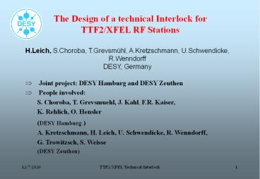
The Design of a technical Interlock for TTF2/XFEL
RF Stations
H.Leich, S.Choroba, T.Grevsmühl, A.Kretzschmann,
U.Schwendicke, R.Wenndorff DESY, Germany
- Joint project DESY Hamburg and DESY Zeuthen
- People involved
- S. Choroba, T. Grevsmuehl, J. Kahl, F.R. Kaiser,
- K. Rehlich, O. Hensler
- (DESY Hamburg )
- A. Kretzschmann, H. Leich, U. Schwendicke, R.
Wenndorff, - G. Trowitzsch, S. Weisse
- (DESY Zeuthen)
2
Main Task of the Interlock Sytem
- Guarantee the operator/other persons safety
- Prevent any damage from the cost expensive
components of the RF station - Also prevent any damage from other environment
- Collect status information of all components of
the RF station and send this information to the
main Slow Control System
Sources of Interlock Error Signals
- Hard component failures (non-reversible hardware
malfunction) - --gt broken cable or damaged contact, dead sensor,
... - Soft errors (e.g. sparks in the klystron or wave
guide system, - temperature above a threshold, ...)
- Error conditions caused by transient noise from
the RF station itself
3
Components of a TTF2/XFEL RF Station
- HV Power Supply
- Provide the input voltage of 1-12 KV to the
capacitor bank of the Modulator - Modulator
- Discharges a fraction of the energy stored in the
capacitor bank into the pulse transformer. A
bouncer circuit will ensure that the 120 kV high
voltage output pulse will be flat i.e. voltage
drop will not exceed some predefined level. - HV Transmission Line
- Connects the Modulator with the pulse
transformer. - Pulse Transformer
- Transforms the 12 kV, 1200 A pulse generated by
the Modulator into a 120 kV, 120 A pulse driving
the Klystron cathode voltage. - Persons and machine safety systems, control
electronics - Several personnel and machine safety systems are
interacting together to provide a safe operation
of the whole system - Low Level RF System (LLRF)
4
Interlock System Architecture
Higher Level Control System (DOOCS)
Interlock Controller
Process Analysis
Output to Process
Strictly hierarchical Architecture
Analog Process Input
Digital Process Input
Analog Output
Digital Output
Adapter Unit
Adapter Unit
Sensor
Sensor
Components of the RF Station
5
(No Transcript)
6
The Implementation
? 19 4U System with dedicated backplane
optimized to the application ? 3U-Eurocard
board format with two 5-Row connectors (CPCI
type) 125 110 235 pins
- enough pin resources per slot and to build a
compact interlock/control system - Front-to-rear connections 40 Pins
- Control Bus 50 Pins
- Time Multiplex Bus 16 Pins
- Service Request lines 20 Pins (one per slave
slot) - Direct Digital Out 24 Pins
- Data throughput
- Control Bus 15 MBytes/s
- Time Mux Bus updates 128 Interlock
Status Signals within 1µs
7
Structure of the Interlock Crate Bus System
8
Interlock Inputs
- Digital Inputs
- - Oil levels
- - Cooling water flow
- Vacuum pump current
- Analog Inputs
- - Oil temperature
- - Cooling water temperature
- - Klystron Filament voltage current
- - Solenoid voltage current
- - SF6 gas pressure
9
Interlock Inputs / Outputs
- Inputs from other Subsystems
- - Persons interlock
- - RF leakage detector
- - Modulator ready
- - Gun interlock
- - RF system ready
- Interlock Outputs
- - Modulator on/off
- - Heater power supply on
- - Klystron solenoid power supply on
- - RF enable
10
Controller Architecture
Cyclone-II EP2C35F484-C7
Flash Memory 32 MByte
NIOS-II 32-Bit RISC CPU
Cntrl Bus Address Out Strb,We Data I/O
SDRAM 64 MByte
Internal SPI Interface
Ethernet Controller
External Devices
Interlock Direct Data Out
Interlock Bus Interfaces Control Bus, Time
Multiplex Bus Service Request lines,
Read Interlock Status, Channel masking,
256 KByte MRAM
Interlock Service Request
Time Mux Bus Address Out Data In
RTC (connected to SPI)
Hardwired Interlock Logic
Data Bus
Address Bus
11
(No Transcript)
12
Components to be tested
Interlock Selftest
- Controller
- Backplane
- Slaves (all installed)
- Power Supply modules and Fans
13
Constraints
- After reset a test of all components is performed
using a special Test Mode (System Test). Two
dedicated bus lines (SysTest_A and SysTest_B)
control the operations in this mode. - If SysTest was successful the system enters the
normal Interlock Mode - In Interlock Mode all components, which are
accessible from the CPU, can be tested (e.g.
periodically when the HV pulse pauses) - Simple logic let the Controllers CPU do most
of the jobs
14
Modul ID Structure
Field type Field name Field length (byte) example
Binary Station number 1 18
Binary A/B-side flag 1 1 (B-side)
ASCII module name 24 Controller
ASCII Version 8 1.2
ASCII Prog. File name 24 Intlk3_cntrl.pof
ASCII Prog. File date 8 051103
15
Interface to the higher level Control System
- The 32-bit RISC processor on the Controller
board performs all necessary control functions to
all slave modules in the interlock crate. The
interface to the DOOCS Control System is
implemented via Ethernet. A TINE server runs on
the NIOS processor and provides an interface to a
DOOCS client. - All status information and all mask data will be
accessible as properties in the context of TINE - All actual values of analog input channels are
implemented as properties - All commands to the interlock crate (to the
controller) are implemented as DOOCS properties
and may be issued by a DOOCS client - The actual values of the data mentioned above are
stored in the DOOCS History Format
16
Web-Server for debugging and maintenance
- A Fail-safe timer on the controller monitors the
TINE-server operations. After it times out (if
the TINE server hangs up or as a result of a
special TINE command) a Web-Server is started
automatically. - The Web-server provides access to all system
resources (status, masks, analog channels) but
also provides the possibility to upload new
software onto the controller and to reprogram the
serial flash device which holds the actual FPGA
configuration. - Only authorized users are able to change flash
content (program flash or FPGA configuration
flash) and/or perform reset operations (Hard- or
Soft-reset)
17
Slave Module Overview
- Digital IO Light Link
- Versatile Link (VL)- or ST- Connectors
- Basic card 4x Input 4x Output max. 2
piggybacks - piggyback either 8x Output (VL)
- or 8x Input (VL)
- or 4x Input 4x Output (VL)
- or 3x Input 3x Output (ST)
18
- Digital Input/Output Module
- 8 Input Groups 2 groups with 8 channels and 6
groups with 4 channels per group - Input Voltage Range 14 V to 40 V
- Switch Detection Threshold typical 3.75 V
- Programmable Wetting Current
- 4 programmable inputs per group to Monitor 4
SwitchtoBattery or 4 Switch-to-Ground Switches - 2 Output Groups with 4 channels per group
- RDS(ON) of 0.55 ? (typical)
- Outputs are current limited (0.8 A to 2.0 A) to
drive incandescent lamps - Output voltage clamp is 45 V and -20 V
(typical) during inductive switching. - Short circuit detect and current limit with
automatic retry - Independent over-temperature protection
- Each group is DC-decoupled from all other groups
and the rest of the board - The module incorporates an interface to the
interlock hardware
19
Analog Input/Output Module
- 4 groups of 4 channels each
- 2 output channels (based on16 bit DAC) and 2
input channels (based on 16 bit ADC) - Voltage range for input and output is 0 10V
- Outputs are buffered to drive 600 O loads
- Conversion rate is 125 kSamples/s
- integrated self test possibility each voltage
output can be connected (via an analog switch) to
a corresponding voltage input - Each group is DC-decoupled from all other groups
and the rest of the board
20
Analog Input Module with Window Comparators
- 36 analog inputs 32 of them are fed via
programmable window comparators - two versions
- current input 4...20 mA Label A
- voltage input 0...10 V Label V
- Sample rate all 36 inputs are updated within 1
ms - Sensor excitation from internal 12 V optional
24 V - Accuracy 0,5 K guaranteed, typically better
than 0,1 K - Resolution for interlock 0,1 K
- Drift with temperature lt 100 ppm which is 0,1
/ 10 K, not compensated - access to all data and control registers via the
Control Bus - This module incorporates an interface to the
interlock hardware
21
TINE Server
22
Interlock WebServer Screenshot 1
23
Interlock WebServer Screenshot 2
24
(No Transcript)
25
(No Transcript)
26
Interlock Crate with Backplane
27
Interlock Controller Board (Final Version)
28
Light Link IO Board (ST-Conn.)
29
Light Link IO Board (Versatile Link)
30
Digital IO Board
31
Analog IO Board
32
Distribution Panel
Recommended
CrystalGraphics Presentations


