
Quasi-adiabatic Clocking and Thermal Effect in Quantum-dot Cellular Automata - PowerPoint PPT Presentation
Title:
Quasi-adiabatic Clocking and Thermal Effect in Quantum-dot Cellular Automata
Description:
Homework Your task is to design a regular structure such as Kronecker Lattice or Shannon Lattice using modern Quantum Dot Cellular Automata technology. – PowerPoint PPT presentation
Number of Views:209
Avg rating:3.0/5.0
Title: Quasi-adiabatic Clocking and Thermal Effect in Quantum-dot Cellular Automata
1
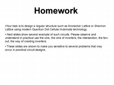
Homework
- Your task is to design a regular structure such
as Kronecker Lattice or Shannon Lattice using
modern Quantum Dot Cellular Automata technology. - Next slides show several example of such
circuits. Please observe and understand in
practical use the wire, the wire of inverters,
the intersection, the fan-out, the way of
creating inverters. - These slides are shown to make you sensitive to
several problems that may occur in practical
circuit designs.
2
Majority Gate and its uses to realize AND and OR
gates.
Smaller inverters will be also shown
3
Majority Gate
Look also to lecture notes for explanation how
this gate works
4
Coplanar wire-crossing
Inverter chain goes vertically
Normal array goes horizontally
5
Inverter
6
Realization of a circuit
7
(No Transcript)
8
(No Transcript)
9
This slide shows how you can use PowerPoint to
create well-aligned to grid figures of wires and
intersection of wires.
10
Homework Continued
- Your task is to design a regular structure such
as Kronecker Lattice or Shannon Lattice using
modern Quantum Dot Cellular Automata technology. - Next slide show an example of such circuit.
Please observe and understand in practical use
the wire, the wire of inverters, the
intersection, the fan-out, the way of creating
inverters. - Please observe the small shift between the left
and right part of the schematics. Explain why it
is done.
11
Shifted down by half cell. Explain why?
12
In this and next slides we give few examples of
QD circuits to show how typical layout/logic
problems are solved.
13
(No Transcript)
14
(No Transcript)
15
S1 S0
16
D Filp-Flop
17
(No Transcript)
18
Barrel Shifter
19
output
Input 1
1
Input 2
0
control
Blue circles represent parts of wires that may be
removed or not, depending on the function that is
realized
Majority configured to OR
This slide shows Shannon cell from a Lattice.
Dimensions are wrong. Please explain how this
works and improve the wiring sizes.
Majority configured to AND
20
- The next slide shows the layout of connections to
the cell in the 33 lattice. - It has not all power of connecting from the
recent paper. - Think how to modify this circuit so that there
will be possible to connections to left, two
connections to top and two connections to right
cells. (in a notation where circuit grows from
bottom to top, here the circuit grows from left
to right).
21
cell
22
Simplified and non-optimized Positive Davio Cell.
Observe how EXOR is realized. Can you find a
better way?
cntr
1
This is Positive Davio Cell without connections
to neighbors. The rules of neighborhood are not
preserved. Correct this circuit and try to
optimize it.
0
exor
23
- Next slide shows a general cell of reconfigurable
FPGA with AND/EXOR cell. This cell can realize
Positive and Negative Davio and Shannon (using
exor). It allows for swapped expansions and for
function A B XOR A B where A denotes
arbitrary polarity of singal A. - In the next slides inverters were not correctly
realized. Think how this can be improved. There
are two ways to realize inverters. Stand-alone
and in wires.
24
cntr
1
0
1
0
25
Final Homework
- Select on of the following and realize preserving
all design rules. - A) Shannon Cell for 22 lattice
- B) Positive Davio Cell for 22 lattice
- C) General Cell for 22 lattice
- D) General Cell for 33 lattice
- E) General Cell for the paper with Mishchenko.
Recommended
CrystalGraphics Presentations


