
Etching and Cleaning - PowerPoint PPT Presentation
1 / 17
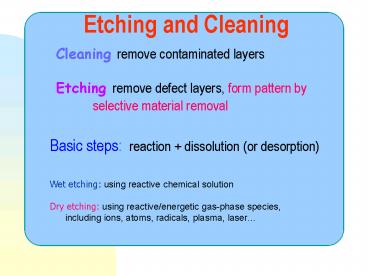
Title: Etching and Cleaning
1
Etching and Cleaning
Cleaning remove contaminated layers Etching
remove defect layers, form pattern by selective
material removal
Basic steps reaction dissolution (or
desorption)
Wet etching using reactive chemical
solution Dry etching using reactive/energetic
gas-phase species, including ions, atoms,
radicals, plasma, laser
2
Patterning by lithography and wet etching
Cr patterned film
Etching of Al film
Mask
transparent glass
photoresist
Si
Al film
SiO2 film
Pattern transfer to photoresist
Si
UV exposure
Develop solution
Si
Si
Si
3
Etchants for Si
4
Isoetch Curves for Si and GaAs
H2SO4H2O2H2O For GaAs
HFHNO3diluent For Si
5
Anisotropic etching
mask
undercut
Isotropic etching
6
Anisotropic etching of Si
Si(100)
Si(110)
7
Wet etching of noncrystalline films
- SiO2 HF NH4F H2O (buffered HF, BHF)
- PSG BHF or HF HNO3 H2O (32150, fast for
PSG) - Si3N4 buffered HF, but very slow
- with H3PO4, rate for Si3N4 SiO2 ? 10 1
- Poly-Si HF HNO3 H2O (3 50 20)
- Al H3PO4 HNO3
- Au and Pt HCl HNO3 (3 1, aqua
regia) - W KH2PO4 KOH K3Fe(CN)6 H2O
8
Undercut in wet etching
Layer 1
Layer 2
Isotropic etching undercut
Film etching undercut
Undercut at interface due to stress
9
Wet etching advantages and disadvantages
- High selectivity, simple facility
- Severe undercut, rough edges, large amount of
chemical waste
Dry etching physical and chemical
- Physical ion bombardment, directional flux
- Chemical reactive atoms, molecules, radicals
- Chemical Physical enhanced reaction/desorption
- by electrons, ions, photons, plasma
10
Etching by Ion Sputtering
Neutralized ion beam good for conductor
insulator
11
Etching by Ion Sputtering
Plasma Sputtering
Weak selectivity in ion beam etching
12
DC RF Sputter Etching
Voltage ratio in RF sputtering VC/VA
(AA/AC)n RF sputtering can be applied to
insulator
13
Chemical Etching Plasma Reactors
Downstream
In situ
Shielded tunnel
14
Reactive Ion Etching (RIE)
Physical Chemical Effects
Deep via holes for inter-level connections
15
Vapor pressure of metal halides
16
Etch chemistry for different materials
- Halogen etching for Si, W, Mo, Ti
- e.g. W 6F ? WF6
- Fluorocarbon (CF4, C2F6, CHF3) for SiO2, PSG,
Si3N4 - e.g. e- CF4 ? CF3 F e- (plasma
dissociation) - 12F Si3N4 ? 3SiF4 2N2
- CF4-H2 mixture increasing HF, reducing F
concentration - Increasing SiO2 etching, decreasing Si and
photoresist - etching
- Cl-based RIE low volatility of SiCl4, desorption
stimulated - by ion and electron flux ? increased
anisotropy - Etching of Aluminum by BCl3, CCl4
17
Etching rate in CF4-H2 plasma
Increasing selectiveity