
CMS HCAL TIMING - PowerPoint PPT Presentation
1 / 21
Title: CMS HCAL TIMING
1
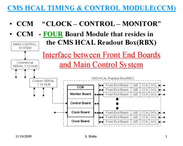
CMS HCAL TIMING CONTROL MODULE(CCM)
- CCM CLOCK CONTROL MONITOR
- CCM - FOUR Board Module that resides in the
CMS HCAL Readout Box(RBX)
Interface between Front End Boards and Main
Control System
2
CMS HCAL TIMING CONTROL MODULE(CCM)
- The purpose of this review is to understand
the current capabilities of the CCM and the
modifications that would be necessary to increase
the modules' functionality. At the end of the
review, I would like to take a decision on the
scope of the CCM repair work we undertake. If we
are not able at the time of the review to make
that decision, I would like to come up with a set
of measurements/tasks and a time table that would
allow us to get to that decision point. J.W.
3
CMS HCAL TIMING CONTROL MODULE(CCM)
- CCM performs three main functions
- 1). Receive and distribute a low skew 40 MHz.
Clock along with a beam-crossing marker to the FE
cards. - 2). Monitor the temperature at the FE cards and
also the power supply voltages that are present
on the backplane. - 3). Provide a means for a Main Control system to
communicate with the ASICs located on the FE
cards and also provide a method to download
parameters to those ASICs in a global manner.
4
HB, HO HE CCM HF(6U VME) does not have
aluminum shell
5
CCM - HB, HO, HEBoard 1 Board 5 Board 3
Board 4
6
CCM Board 1
7
CCM Board 5
8
CCM Board 3
9
CCM Board 4
10
Documentation
- http//www-ppd.fnal.gov/holm.myweb/CMS_HCAL.htm
- http//www-ppd.fnal.gov/holm.myweb/CCM_V4_Document
ation.htm - Web pages contain
- Board Schematics
- FPGA Design Top Level Block Diagram VHDL code.
- Operation and Communication Protocol
- Modification note for the A/D readback
- Diagram showing clock modification for HF
- Excel file showing cost of producing new Board 5
11
Known problems
- A/D Problem
- During the design phase a timer within the FPGA
that controls the Analog Mux and A/D converter
was reduced to eliminate logic within the
FPGA.The timer allowed for a longer time between
conversions which allowed the signal connected to
the A/D to stabilize. - The A/D has an input impedance input of 10K, the
resistor connected to the Temperature Sensor
gives a high output impedance of 6.65K. When the
Analog Mux selects an input port the parallel
combination of the two impedances drops the
resistance thus changing the voltage
drop(temperature sensor current remains the
same). Also the analog switch has a drain
capacitance of 200pf when the switch is closed
the current from the temperature sensor(or charge
stored in source capacitance) must
charge/discharge the 200pf to the correct value
in 2us. - Adding a unity gain buffer between the Analog
Mux output and the A/D input removes the offset
from the parallel combination and provides a high
impedance input to the temperature sensor and a
low impedance output to the A/D.
12
- A/D modification
- FPGA is OTP it cannot be changed.
- Add a Unity Gain Buffer between Analog Mux and
A/D Convertor - 0.1uf Capacitors to the Analog Mux Inputs to
stabilize the inputs. - Changed the Resistor Value on voltage divider for
the V2 voltage measurement. - Disconnected the Input Mux channel that was
measuring ground and connected to adjacent
channel. - With all inputs setting at approximately the same
value a large change in a input voltage can be
detected. - A missing or defective sensor cannot be detected.
13
Scope picture of A/D input11us per channel, T3
2M resistor to gnd
V1
V2
T1
T2
V2
T4
T5
T6
TCCM
V1
T3
14
Scope picture of A/D input11us per channel, T3
Floating
V1
V2
T1
T2
V2
V1
V2
T1
T2
V2
T4
T5
T6
TCCM
V1
T3
T4
T5
T6
TCCM
V1
T3
15
Scope picture of A/D input11us per channel, T2
Heated, T3 Floating
V1
V2
T1
T2
V2
V1
V2
T1
T2
V2
V1
V2
T1
T2
T3
V2
T4
T5
T6
TCCM
V1
T3
T4
T5
T6
TCCM
V1
T4
T5
T6
TCCM
V1
T3
16
- QIE RESET Problem
- QIE reset signal from CCM is not synchronized to
the FE boards clock. - -Scoopshot slide3 (QIE reset but no LED)I have
my trigger on the L1A (Blue channel3)I can see
the long or b-channel modulation in the clock (in
yellow)every event.There is a QIE-reset on
backplane (in green)but no pindiode signal from
HF calibration unit (in yellow on the leftbottom
corner).
17
CMS HCAL TIMING CONTROL MODULE(CCM)
HCAL FE simplified scheme of reset and TTC logic
CCM ACTEL FPGA
GOL
DIN(24)
RESET_PLL
Brcst4
pll_reset
pll_reset
RESET_b (gt13us of IDLE frames)
RESET_PLL-
TX_EN
TX_ER
CCA
SEND_FF
Brcst2
TX_SEND_IDLE
QIE_RESET
QIE_reset
FF
Slow Controls
RST_DLL
used only inside the CCA
RESET
FE_RESET
gen_reset
RST_CCA
RESET-
QIE_RESET
FPGA Clock
Brcst2
QIE
QPLL2
FE Board Clock A
RESET (generate the 70-ticks orbit message)
QPLL1
FE Board Clock B
TTCrx
QPLL2
Backplane
18
CMS HCAL TIMING CONTROL MODULE(CCM)
MODIFIED HCAL FE simplified scheme of reset and
TTC logic
CCM ACTEL FPGA
GOL
DIN(24)
RESET_PLL
Brcst4
pll_reset
pll_reset
RESET_b (gt13us of IDLE frames)
RESET_PLL-
TX_EN
TX_ER
CCA
SEND_FF
Brcst2
TX_SEND_IDLE
QIE_RESET
QIE_reset
FF
Slow Controls
RST_DLL
used only inside the CCA
RESET
FE_RESET
gen_reset
RST_CCA
RESET-
QIE_RESET
FPGA Clock
Brcst2
QIE
QPLL2
FE Board Clock A
RESET (generate the 70-ticks orbit message)
QPLL1
FE Board Clock B
TTCrx
QPLL2
Backplane
19
- FPGA CLOCK Modification
- Synchronizes the QIE reset signal to the same
clock that the FE boards use. - Change the FPGA Clock from the QPLL1 source to
the TTCrx Clock. - If TTCrx clock is absent it removes the
possibility of communication with the CCM FE
boards.
20
- Other Changes ?
- Has the CCM been used enough at this time to say
that there are not other changes needed?
21
CMS HCAL TIMING CONTROL MODULE(CCM)
- Considerations
- Cost of making a new board 5
- 70k for 200 boards all new parts
- 60k using left over parts from 1st run that
are spares - Radiation Qualification of new lots of parts (?)
- Time