
The Development of Large-area Pico-sec Resolution Time-of-flight - PowerPoint PPT Presentation
1 / 38
Title:
The Development of Large-area Pico-sec Resolution Time-of-flight
Description:
The Development of Largearea Picosec Resolution Timeofflight – PowerPoint PPT presentation
Number of Views:36
Avg rating:3.0/5.0
Title: The Development of Large-area Pico-sec Resolution Time-of-flight
1
The Development of Large-area Pico-sec Resolution
Time-of-flight
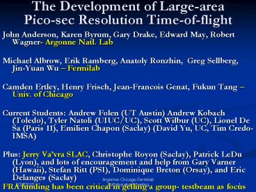
- John Anderson, Karen Byrum, Gary Drake, Edward
May, Robert Wagner- Argonne Natl. Lab - Michael Albrow, Erik Ramberg, Anatoly Ronzhin,
Greg Sellberg, Jin-Yuan Wu Fermilab - Camden Ertley, Henry Frisch, Jean-Francois Genat,
Fukun Tang Univ. of Chicago - Current Students Andrew Folen (UT Austin) Andrew
Kobach (Toledo), Tyler Natoli (UIUC/UC), Scott
Wilbur (UC), Lionel De Sa (Paris 11), Emilien
Chapon (Saclay) (David Yu, UC, Tim Credo-IMSA) - Plus Jerry Vavra SLAC, Christophe Royon
(Saclay), Patrick LeDu (Lyon), and lots of
encouragement and help from Gary Varner (Hawaii),
Stefan Ritt (PSI), Dominique Breton (Orsay), and
Eric Delanges (Saclay) - FRA funding has been critical in gelling a group-
testbeam as focus
2
Motivation for Psec TOF-1
- High Energy Colliders are major investments- we
should use them as efficiently as possible. - Information in collisions is of (only) 3 types
- 4-vectors (E, p)gt mass and 3-vector momentum
- Vertices (including lifetimes)
- Spins (leptons, baryons only)
- 1 psec is 300 microns in path lengthgt 3rd coo
(x,y,z) - Measure velocity by TOF, momentum by tracking gt
get mass gt get quark content - Work up the flavor tree s to c to b to t
- Example top decay W-gtcsbar, udbar b vs bbar
3
A real CDF Top Quark Event
T-Tbar -gt WbW-bbar
Measure transit time here (stop)
W-gtcharm sbar
B-quark
T-quark-gtWbquark
T-quark-gtWbquark
B-quark
Cal. Energy From electron
- Fit t0 (start) from all tracks
W-gtelectronneutrino
Can we follow the color flow through kaons,
charm, bottom? TOF!
4
Geometry for a Collider Detector
2 by 2 MCPs
Beam Axis
Coil
- r is expensive- need a thin segmented detector
5
Idea 1 Generating the signal
- Use Cherenkov light - fast
Incoming rel. particle
Custom Anode with Equal-Time Transmission Lines
Capacitative. Return
A 2 x 2 MCP- actual thickness 3/4 e.g. Burle
(Photonis) 85022-with mods per our work
Collect charge here-differential Input to 200 GHz
TDC chip
6
Major advances for TOF measurements
Micro-photograph of Burle 25 micron tube- Greg
Sellberg (Fermilab)
- 1. Development of MCPs with 6-10 micron pore
diameters
7
Motivation for Psec TOF-2
- Vertexing photons at the LHC- at present its
hard to know if a high-Pt photon comes from the
same vertex as the rest of the event. Radiator in
front of TOF know velocity time gives distance
to vertex (1psec300 micron swath along arc swung
from photon) - Example high-profile LHC analyses
- (Jim Pilcher) Higgs-gt gamma-gamma
reconstructing the mass using the right vertex - Rare events- e.g. photino decays- associating the
photon with the right vertex and decay products - Long-lived objects decaying to photons- find
delayed photons (e.g. Maxs photons at CDF)
8
Motivation for Psec TOF-3
Toback ,Goncharov et al- CDF
- Separating Multiple Vertices at High Luminosity
at the LHC - Small crossing diamond (s7 cm) many
interactions/crossing - Happen at different places AND different times
(can be head-tail or tail-head OR head-head or
tail-tail, respectively)- use 2D plot to separate
vertices - (interesting and little known fact- interactions
happen earlier in the east than in the west in
B-zero- puzzle for the student)
9
Motivation for Psec TOF-4Other uses
- 1. Diffractive Higgs production (missing mass)-
Totem, AFP at LHC (Albrow, Royon, et al) - 2. Muon cooling studies- e.g. MANX 6D cooling
- 250 MeV muons- lazy objects. Measure
direction and velocity before cooling, direction
and velocity after coolinggt dont need 2
magnetic spectrometers. (Rol Johnson, Tom
Roberts, Muons.Inc et al.) - 3. LHCb-geometry- forward photon and charged TOF
- 4. Water Cherenkov water-TPC (Howard
Nicholson)- if can make VERY large area TOF with
few mm and 50 psec resolution do 3D ring-imaging
can reconstruct track direction from time of
photons
10
FY-08 Funds- Fermilaba) Testbeam capability b)
Electronics c) LHC Higgs mm search
- Purchase of microchannel plate PMTs, constant
fraction discriminators, 14 bit ADCs, for
support of international test beam experiment
T979 at the Meson Test Beam Facility (Erik
Ramberg) - Component and circuit board purchase for
development of cheap FPGA based TDCs, with 20
psec resolution (Jin-Yuan Wu) - Purchase of specialized isochronous Cerenkov
radiators for an alternative scheme for the LHC
FP420 forward proton time-of-flight detector.
(Mike Albrow)
11
FY-08 Funds FermilabLaser teststand for SiPM
development (Anatoly Ronzhin)
1 photo-electron
4 phes
Laser calibration system to test SiPMs
32 phes
256 phes
12
FY-08 Funds ChicagoAnode Design and
Simulation(Fukun Tang)
- Transmission Line- readout both endsgt pos and
time - Cover large areas with much reduced channel
account.
13
FY-08 Funds ChicagoAnode Design and
Simulation(Fukun Tang)
- Transmission Line- simulation shows 3.5GHz
bandwidth- 100 psec rise (well-matched to MCP) - Board has been made-
14
FY-08 Funds ChicagoPsec-resolution
Multi-channel Front-End Electronics and
Simulations(Jean-Francois Genet, Fukun Tang,
HJF,Gary Varner)
- Left- 200 GHz VCO chip in IBM 8HP bipolar
- Right- new design fast sampling/slow A-to-D
- Advantages- low power, mainstream process (0.13
micron CMOS), CERN, Saclay collab/tools
15
FY-08 Funds ChicagoPsec-resolution
Multi-channel Front-End Electronics and
Simulations(Jean-Francois Genet, Fukun Tang,
HJF,Gary Varner)
- Simulations- include MCP measured signal, noise,
electronics white noise, digitization, analog
bandwidth
Table 1. State of the art, this proposal. The
yellow column is from Gary Varners group at the
University of Hawaii (USA) 12, the light blue
from Dominique Breton from the University of
Paris-Sud (Orsay) 10 and Eric Delagnes from CEA
(Saclay), (France) 11. The orange column
from Stefan Ritt at PSI (Switzerland) 13. The
dark blue is this proposal.
16
FY-08 Funds ANLLaser Test Stand at Argonne
Hamamatsu PLP-10 Laser (Controller w/a laser
diode head) 405 635nm head. Pulse to pulse
jitter lt 10psec (Manufacture Specs)
Electronics
Lens to focus beam on MCP
Diaphram with shutter to next box
MCP 2
Mirrors to direct light
Mirrors to delay light
50/50 beam splitter
X-Y Stager
Laser Head
MCP 1
17
Electronics
Ortec AD114 (14 bit ADC)
Ortec 566
Ortec 9327 AMP/CFD
Stop
Start
Impeccable Instruments Psec Pulser
The intrinsic jitter of the system is 4ps and it
has a resolution of 3.13ps.
FY-08 Funds ANLLaser Test Stand at Argonne
Hamamatsu PLP-10 Laser Diode
18
Timing Resolution Studies
FY-08 Funds ANLLaser Test Stand at Argonne
Histogram using the 635nm laser set at 55pe.
Histogram using the 408nm laser set at 50pe.
The Mark-P and the commercial tube, both 64-anode
25-micron pore tubes with a commercially
available collection scheme were used to find a
limit on the timing resolution. The system was
calibrated before the measurements were taken.
19
FY-08 Funds ANLLaser Test Stand at Argonne
We have measured the timing properties of two
MCP-PMs from Photonis. SLAC Two 64-anode
10-micron pore tubes with commercial charge
collection scheme. Pilas Laser at 635nm.
ARGONNE Two 64-anode 25 micron pore tubes with
commercial charge collection scheme. Hamamatsu
Laser at 408 635nm.
J. VaVras Laser Lab at SLAC
ARGONNE LASER LAB
20
Jerrys Numbers
- TTS 3.8 psec (from a TTS of 27 psec)
- Cos(theta)_cherenk 3.3 psec
- Pad size 0.75 psec
- Electronics 3.4 psec
21
Development
- TTS 3.8 psec (from a TTS of 27 psec)
- MCP development- smaller pores, smaller
gaps, filter chromaticity, diamond ring, ..
Alternative PDs (e.g. Paul Hs diamond) - Cos(theta)_cherenk 3.3 psec
- Same shape- spatial distribution (e.g.
strips measure it) - Pad size 0.75 psec-
live
with it - Electronics 3.4 psec
fast sampling- should be able to get lt 1psec
22
Simulation and Measurement
- Need a serious effort on simulation to
complement measurements - Need a serious collaboration with industry to
make next generations of photo-detectors - Have the electronics we need to understand small
numbers of channels at psec level- larger numbers
at 5 psec level - Are forming a community, but need to generate
long-term funding and support for the idea of
detector RD and also flavor following
23
FY-09 Funds- Fermilaba) Testbeam capability b)
Electronics c) LHC Higgs mm search
- Fast small MCPs for LHC diffractive Higgs search
(Albrow scheme for 1 psec resolution (!)) - Electronics readout for latter
- Extend test-beam capability- new (Roden) MCPs
- FPGA development work- prototoypes
24
FY-09 Funds- Argonnea) Laser Teststand b)
Electronics System clock, FPGA for sampling
testbeam
- Laser teststand is a facility for use by ANL,
Fermilab, UC and others- still some
development/refinement to be done - ANL played a critical role in DAQ system for
test-beam run (going on now- 2nd wk as parasitic
friends)- some more engineering/software to be
done - John Anderson has solved the system clock issues
in principle- would like to implement (also light
source interest) - John and Gary did FPGA for 200 GHz Bipolar
readout- need to adapt for sampling - Have an LDRD proposal in at ANL for ALD but
doesnt cover the tasks listed here- more in the
future
25
FY-09 Funds- Chicagoa) 40 GHz sampling
electronics b) Anode transmission lines c) Test
Beam
- FRA-FY08 has supported writing a proposal for
funding for ASIC development- have all 4 teams as
collab/advisors- seed funding will support
finishing the proposal stage - Have 1st prototype transmission line board from
FY08 funding- will test (laser first)- have plans
for 2nd and 3rd (bigger area, capacitive
coupling) - Anode/transmission line connection still in
proto-type stage (Sellberg, Tang, Ertly, HF)-
development costs (BEST in Rolling Hills).
26
FY-08 Funds ChicagoAnode Design and
Simulation(Fukun Tang)
27
Atomic Layer Deposition
- ALD is a gas phase chemical process used to
create extremely thin coatings. - Current 10 micron MCPs have pore spacing of
10,000 nm. Our state of the art for Photonis MCPs
is 2 micron (although the square MCPs are 10
micron). - We have measured MCP timing resolution and know
it depends strongly on pore size, and should
improve substantially with smaller pores. - M.Pellins group routinely purchase 60nm
micro-channel pores and using ALD have achieved
10nm (this is the state of the art) - UChicago simulations have shown the electronics
contribution can be made substantially less than
a psec.
M.Pellin, MSD
28
Detector Sensor RD Program We are proposing to
use material science expertise at ANL to move
beyond commercially-available MCP devices.
H.Frisch
Cartoon drawings showing the custom atomic-layer
disposition, the small pores, and the custom
anode configuration (left) and our proposed
module frame (right)
29
Summary
- This has gone from a hobby with an IMSA high
school student (Credo) to a nascent program - We have made a number of false starts and wrong
turns (e.g. the IBM bipolar 200 GHz electronics),
but the fundamentals look good- dont see a hard
limit yet. - Have formed an international community- 2
workshops per year (France and Chicago)- includes
companies (Photonis, Photek, IBM) - Have now formed a strong ANL-Fermilab-UC
collaboration centered on the testbeam - Are at the stage where we can apply for
longer-term funding using 1 more year of FRA
support
30
Thats All
31
Backup Slides
32
C haracteristics we need
- Feature size lt 300 microns
- Homogeneity (ability to make uniform large-area)
- Fast rise-time and/or constant signal shape
- Lifetime (rad hard in some cases, but not all)
- System cost ltlt silicon micro-vertex system
33
K-Pi Separation over 1.5m
Assumes perfect momentum resolution (time res is
better than momentum res!)
1 Psec
34
Engineering Highlights
- F.Tang (UChicago) designed Voltage Control
Oscillator using IBM 0.13um SiGe BiCMOS8HP - More challenging - Time Stretcher chip (including
ultra low timing jitter/walk discriminator
dual-slope ramping time stretching circuits etc.) - From simulations, accuracy not good enough (5-10
psecs) F.Tang - Power concerns
- NEW Invented 2 new schemes - a) Multi-threshold
comparators, b) 50 GHz 64-channel waveform
sampling. Both schemes give energy and leading
edge time. - Current plan Save waveform and use multiple
thresholds to digitize. Use CMOS (J.F. Genat,
UChicago) - Dec meeting at UChicago with UChicago, ANL,
Saclay, LBL Hawaii, IBM and Photonis
35
MCP Best Results
- Previous Measurements
- Jerry Vavra SLAC (Presented at Chicago Sep 2007)
- Upper Limit on MCP-PMT resolution s MCP-PMT 5
ps - Takayoshi Ohshima of University of Nagoya
(Presented at SLAC Apr 2006) - Reached a s MCP-PMT 6.2ps in test beam
- Using two 10 um MCP hole diameter
- PiLAS red laser diode (635 nm)
- 1cm Quartz radiator (Npe 50)
Burle/Photonis MCP-PMT 85012-501 (64 pixels,
ground all pads except one)
- Use 2 identical 6 micron TOF detectors in beam
(Start Stop) - Beam resolution with qtz. Radiator (Npe 50)
36
RD of MCP-PMT Devices
- We are exploring a psec-resolution TOF system
using micro-channel plates (MCP's) incorporating
- A source of light with sub-psec jitter, in this
case Cherenkov light generated at the MCP face
(i.e. no bounces) Different thicknesses of
Quartz Radiator - Short paths for charge drift and multiplication
Reduced gap - A low-inductance return path for the
high-frequency component of the signal - Optimization of the anode for charge-collection
over small transverse distances - The development of multi-channel psec-resolution
custom readout electronics directly mounted on
the anode assembly ASIC, precision clock
distribution - Smaller pore size Atomic Layer Deposition
37
(No Transcript)
38
(No Transcript)
Recommended
CrystalGraphics Presentations


