
NIST Nanofabrication Facility - PowerPoint PPT Presentation
1 / 7
Title:
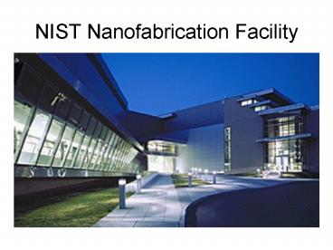
NIST Nanofabrication Facility
Description:
Spectroscopic ellipsometer for thin film thicknesses and optical properties ... Post-processing - to finish up your devices. CNST Nanofab tools (cont.) Using ... – PowerPoint PPT presentation
Number of Views:110
Avg rating:3.0/5.0
Title: NIST Nanofabrication Facility
1
NIST Nanofabrication Facility
2
CNST Nanofab
A state-of-the-art shared-use facility for the
fabrication and measurement of nanostructures
- 19,000 sq ft cleanroom (8,000 sq ft class 100)
- Advanced lithography and microscopy
- Talented staff to train users or operate the
tools - Makes available the expensive tools needed for
nanotechnology - Instrumentation both inside and outside the
cleanroom - Open to all users, NIST and worldwide
3
The CNST Nanofab is well equipped and
expandingSee cnst.nist.gov for details
4
CNST Nanofab tools
Lithography to pattern your chip
- State-of-the-art electron-beam lithography
features as small as 5 nm, across whole wafer - Laser direct-write for mask making and rapid
prototyping - Contact aligners for photolithography
- Focused ion-beam tool for nanoscale milling and
addition of material - Nanoimprint lithography for replicating nanoscale
features
Deposition, oxidation, and diffusion to add
dielectrics, dopants, metals
- LPCVD furnaces for silicon nitride and
poly-silicon - PECVD for low temperature oxides and nitrides
- CMOS-clean or general use furnaces for oxidation
and diffusion doping - Rapid thermal annealing
- Sputter deposition, including dielectrics,
metals, magnetic materials and multilayers - Electron-beam and thermal evaporation
- Atomic layer deposition for molecular-scale,
highly conformal coatings of metals and
dielectrics. - Parylene deposition tool for conformal,
bio-compatible polymer coatings
5
CNST Nanofab tools (cont.)
Etching - to selectively remove material
- Two reactive ion etchers for thin metals and
dielectrics - Two inductively coupled plasma etchers for deep
silicon etching and metal etching - Two special purpose etchers allowing novel
recipes for III-V materials and exotics - Cryogenic and high temperature capability
- Xenon difluoride for sacrificial etching of
silicon for MEMS applications - Microwave ashing for resist stripping
Inspection and metrology to see what you got
- Field-emission scanning electron microscope (SEM)
for high resolution imaging - Tabletop SEM for rapid inspection
- Optical microscopes
- Spectroscopic ellipsometer for thin film
thicknesses and optical properties - Reflectometer for film thickness
- Profilometer for 2D profiling
- Atomic Force Microscope (AFM)
- Wafer curvature tool for measurement of stress
- Four point probe systems for electrical
characterization
6
CNST Nanofab tools (cont.)
Post-processing - to finish up your devices
- Wafer Dicing Saw-Disco Model 341
- Wire Bonder Kulicke and Soffa Model 4526
- Critical Point Dryer
See this list and more at cnst.nist.gov
7
Using the CNST Nanofab
- The Nanofab is fee-based, shared-use
- Based on highly successful NNIN Nanocenter model
- No proposal needed simple one-page description
of work - Open to all users
- NIST site access restrictions apply
- The Nanofab will train users in tool use
- Alternatively, the process can be performed by a
process engineer at an additional cost - Fees are based on operating costs
- Similar to the full cost recovery fees of the
NNIN-NSF Nanocenters - External users may apply to have a portion of
their fee waived - For research supportive of CNST goals
- Net charges similar to NNIN-NSF academic rates
- User can maintain IP rights under certain
circumstances - For information about use of the Nanofab
- Contact Dr. Tony Novembre, the Nanofab Facility
Group Leader (novembre_at_nist.gov) - Contact Dr. Alex Liddle if a joint research
project is more appropriate (liddle_at_nist.gov)
Recommended
CrystalGraphics Presentations


