
EE 5349 Section 5 Microsystems - PowerPoint PPT Presentation
1 / 22
Title:
EE 5349 Section 5 Microsystems
Description:
We study the scaling of mechanical, electrical, thermal, optical and fluidic ... Prior to 1987, these micromechanical structures were limited in motion. ... – PowerPoint PPT presentation
Number of Views:115
Avg rating:3.0/5.0
Title: EE 5349 Section 5 Microsystems
1
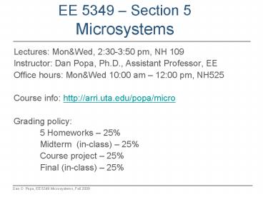
EE 5349 Section 5 Microsystems
- Lectures MonWed, 230-350 pm, NH 109
- Instructor Dan Popa, Ph.D., Assistant Professor,
EE - Office hours MonWed 1000 am 1200 pm, NH525
- Course info http//arri.uta.edu/popa/micro
- Grading policy
- 5 Homeworks 25
- Midterm (in-class) 25
- Course project 25
- Final (in-class) 25
2
Syllabus
- Part 1 Introduction to small things
- Week 1 August 24, 26, Lectures 1, 2
- Introduction to microsystems, brief history.
- Example MST classification and examples.
- Modeling of microsystems - what is different
(scaling laws)? - Week 2 August 31, September 2 Lectures 3, 4
- Modeling Refresher in continuum mechanics
mechanics of beams, plates, statics, dynamics,
electrostatics, electromagnetics, fluid dynamics,
heat conduction, MATLAB simulation. - Week 3 September 9, Lecture 5
- Modeling More on scaling laws.
- Homework 1 posted September 9.
- Week 4 September 14, 16, Lectures 6,7
- - Modeling More on scaling laws.
- Week 5 September 21, 23, Lectures 8,9
- Fundamental concepts in precision design
kinematics, constraints, alignment, flextures,
error compensation, nanometric measurement
principles - Homework 2 posted on September 23.
3
Syllabus
- Part 2 Microfabrication
- Week 6 September 28, 30, Lectures 10,11
- Fabrication Basics of Lithography, Wet and Dry
Etching and Deposition - Examples Micromachined devices.
- Week 7 October 5, 7 Lectures 12,13
- Fabrication EDM and Laser Micromachining.
- Homework 3 posted on Oct. 7
- Week 8 October 12, 14 Lectures 14,15
- Fabrication LIGA and Micromolding.
- Homework 3 posted on Oct. 7
- Week 9 October 19, 21 Lectures 16,17
- Fabrication Surface Micromachining
- Homework 4 posted on Oct 21
- Midterm 1 (in class), October 21
4
Syllabus
- Part 3 Modeling and Control of Microactuators
- Week 10 October 26, 28 Lectures 18, 19
- Modeling Microsystems layout basics design
rules, tools, formats, examples. - Modeling Microsystems modeling and simulation
tools. - Week 11 November 2, 4 Lectures 20, 21
- Modeling Simulation of Microactuators using
SUGAR. - Modeling Reduced Order MEMS Models,
Eectrothermal microactuators. - Homework 5 posted Nov. 4
- Week 12 November 9, 11, Lectures 22, 23
- Modeling Electrostatic Microactuators and
MEMS Control - Week 13 November 16, 18, Lectures 24, 25
- Modeling Piezoelectric, SMA, and Magnetic
actuators
5
Syllabus
- Part 4 Microassembly, Micropackaging
- Week 14 November 23, 25, Lectures 26, 27
- Backend Introduction to microassembly and
microrobotics. - Example Microfluidic and Microoptical systems.
- Week 15 November 30, December 2, Lectures 28,
29 - Backend Introduction to microsystems packaging.
- Course project due Dec. 2 with presentation
- Week 16 December 7, 11
- Final Exam (In-class, comprehensive) Dec 7.
6
Syllabus
- Grading policy on curve
- Homeworks 5. Homeworks contain both written
and/or computer simulations using MATLAB. Submit
code if it is part of the assignments. - Reading Assignments After each course. The
assigned reading material is given out in order
to make you better understand the concepts.
Materials from the reading assignments may be
part of course exams. - Examinations One midterm (in class) and one
final (in class). - Course project Due on Dec 2, with a report and
an in-class presentation. This project requires
students to focus on a microsystem from a list
provided in class, and walk through details
related to its manufacturing and
characterization. Students should identify
suitable materials, designs, models, and
processes to manufacture the microsystem and
report their findings in a 8-10 page research
report.
7
Textbooks
- Modeling MEMS and NEMS, by J.A. Pelesko, D. H.
Bernstein, Publisher ChapmanHall/CRC Press,
2003, ISBN 1-59488-306-5 (required) - Fundamentals of Microfabrication, by Marc J.
Madou, Second Ed., Publisher CRC Press, 2002,
ISBN 0-8493-0826-7 (required) - Microsystem Technology and Microrobotics, by S.
Fatikow, U. Rembold, Publisher Springer-Verlag,
1997, ISBN 3-540-605658-0 (recommended, on
library reserve) - Fundamentals of Microsystems Packaging, by Rao
Tummala (Ed.), Publisher McGraw Hill, 2001,
ISBN 0-07-137169-9 (recommended, on library
reserve) - Foundations of Ultraprecision Mechanism Design,
by St. Smith, D.G. Chetwynd, Publisher CRC
Press, 1992, ISBN 2-88449-001-9 (recommended, on
library reserve) - Fundamentals and Applications of Microfluidics,
Second Edition (Integrated Microsystems), by
Nam-Trung Nguyen, Steven T. Wereley, Publisher
Artech House Publishers, 2006, ISBN 1580539726
(recommended, on library reserve)
8
Course Tools
- Math linear/matrix algebra, trigonometry,
differential equations (ODE and PDE). - Physics thermodynamics, mechanics of plates,
electrostatics. - Programming MATLAB.
- UC Berkeley SUGAR 2.0 for MATLAB, available for
download - http//www-bsac.eecs.berkeley.edu/cadtools/sugar/s
ugar
9
Honor Code
- Missed deadlines for take-home exams and
homeworks Maximum grade drops 10 per late day.
Speak to me about missed deadlines for full
credit in extenuating circumstances. - Academic Dishonesty will not be tolerated. All
homeworks and exams are individual assignments.
Your take-home exams and homeworks will be
carefully scrutinized to ensure a fair grade for
everyone. - Attendance and Drop Policy Attendance is not
mandatory. However, if you skip classes, you will
find the homework and exams more difficult.
Assignments are going to be posted here, however,
due to the pace of the lectures, copying someone
else's notes may be an unreliable way of making
up an absence. You are responsible for all
material covered in class regardless of absences.
10
Lecture 1 Intro to Microsystems
- Course Outline
- Microsystems vs. MEMS.
- Brief history.
- Basic concepts what this course covers.
11
What is a microsystem?
- A system with dimensions generally between 1µm
and 1mm at the functional device level, and 1mm
to 1cm at the system level. - System scaling Expressed in terms of part size,
tolerance or positioning accuracy. Definition
taking into account the types of instruments
needed for visualization. - Nano Part sizes below 500nm, positioning
accuracy below 250nm, SEM/TEM. - Micro Part sizes between 0.5 µm and 500 µm,
accuracy between 0.25 µm and 2.5 µm, optical
microscope. - Meso Part sizes between 500 µm and 5 cm,
accuracy between 2.5 µm and 25 µm, regular
optics. - Macro Part sizes greater than 5 cm, accuracy
greater than 25 µm, regular optics. - Special cases where not all 3 dimensions are in
the same size scale, for example optical fibers
or thin substrates.
12
Microsystems examples
- Examples in nature abound
- living cells
- capillary blood vessels
- small insects (e.g. fruit fly)
- Examples of older man-made systems
- Watches
- Microdrills at your dentist office
- Thin films for your sunglasses
- Examples of recent man-made microsystems
- Microfluidic microTAS (Lab-on-Chip).
- Microoptic micromirror array (DMD).
- Micromechanic microaccelerometers (air-bags).
- Microsensors gas and pressure transducers.
13
Why small is different
- Micromachines are governed by the same physical
equations as macromachines, but solutions of
these equations have different dominant effects. - These effects sometimes work in favor of a
microsystem (for instance devices are lighter,
faster, consume less power). Sometimes they work
against MST (less force, harnessing less power,
etc). - Quantifying these effects is done though
so-called scaling laws, where the variable of
interest (e.g. mass, power, temperature, force)
is expressed in terms of the device scale - OutputKrn, n scaling factor, r device length
scale, K- constant. - Most important scaling law is a result of the
ratio between surface and volume. At small
scales, surface effects become dominant. - V4/3?r3, A?r2, V/AO(r), therefore VltltA if
rltlt1. - Example of surface effects electrostatic
attraction of plates - Example of volumetric effects gravitational
force. - In this course we will look at solutions
governing the evolution of microsystems and
derive appropriate approximations for their
length scales. We study the scaling of
mechanical, electrical, thermal, optical and
fluidic physical laws.
14
Microsystems VS. MEMS
- MEMS/MOEMS Microelectromechanical,
Microoptoelectromechanical systems - Term coined in the 1980s in the US using
fabrication technology similar to the IC
semiconductor industry. - MST Microsystems Technology
- Terms used mostly in Europe to denote
miniaturized devices and associated technology. - Micromachines
- Term used mostly in Japan to denote miniaturized
machines and systems, including those used to
manufacture. - MEMS is a subset of MST, as it includes
- Non-Silicon materials
- Non-IC fabrication methods
- Precision engineering concepts
- In this course we focus on MST rather than just
MEMS.
15
Why making small things is a lot harder than
making conventional things
16
Brief History of Microsystems (USA)
- Invention of the transistor at Bell Telephone
Laboratories in 1947 sparked a fast-growing
microelectronic technology. Jack Kilby of Texas
Instruments built the first integrated circuit
(IC) in 1958 using germanium (Ge) devices. It
consisted of one transistor, three resistors, and
one capacitor. The IC was implemented on a sliver
of Ge that was glued on a glass slide. Later that
same year Robert Noyce of Fairchild Semiconductor
announced the development of a planar
double-diffused Si IC. The complete transition
from the original Ge transistors with grown and
alloyed junctions to silicon (Si) planar
double-diffused devices took about 10 years. The
success of Si as an electronic material was due
partly to its wide availability from silicon
dioxide (SiO2) (sand), resulting in potentially
lower material costs relative to other
semiconductors. Since 1970, the complexity of ICs
has doubled every two to three years. The minimum
dimension of manufactured devices and ICs has
decreased from 20 microns to the sub micron
levels of today. Current ultra-large-scale-integra
tion (ULSI) technology enables the fabrication of
more than 10 million transistors and capacitors
on a typical chip. - Richard Feynman delivers his famous lecture
There is Plenty of Room at The Bottom, in which
he notes that in 40 years from now. Feynman
considered a number of interesting ramifications
of a general ability to manipulate matter on an
atomic scale. He was particularly interested in
the possibilities of denser computer circuitry,
and microscopes which could see things much
smaller than is possible with scanning electron
microscopes. These ideas were later realized by
the use of the scanning tunneling microscope
(1982) and the atomic force microscope (1986).
Feynman also suggested that it should be
possible, in principle, to do chemical synthesis
by mechanical manipulation, and he presented the
"weird possibility" of building a tiny,
swallowable surgical robot by developing a set of
one-quarter-scale manipulator hands slaved to the
operator's hands to build one-quarter scale
machine tools analogous to those found in any
machine shop. - K. Eric Drexler reuses Feynmans ideas in the
context of Molecular Manufacturing in 1981. He
introduced the concept of a billion tiny
factories and added the idea that they could make
more copies of themselves, via computer control
instead of control by a human operator, in his
1986 book Engines of Creation The Coming Era of
Nanotechnology. Carbon nanotubes were invented
prior to Sumio Iijimas Nature paper that brought
them in focus in 1991, and mass-produced in 1996
by Richard Smalley at Rice University.
17
Brief History of Microsystems (USA)
- Attention was first focused on microsensor (i.e.,
microfabricated sensor) development. The first
microsensor, which has also been the most
successful, was the Si pressure sensor. In 1954
it was discovered that the piezoresistive effect
in Ge and Si had the potential to produce Ge and
Si strain gauges with a gauge factor (i.e.,
instrument sensitivity) 10 to 20 times greater
than those based on metal films. As a result, Si
strain gauges began to be developed commercially
in 1958. The first high-volume pressure sensor
was marketed by National Semiconductor in 1974. - Around 1982, the term micromachining came into
use to designate the fabrication of
micromechanical parts (such as pressure-sensor
diaphragms or accelerometer suspension beams) for
Si microsensors. The micromechanical parts were
fabricated by selectively etching areas of the Si
substrate away in order to leave behind the
desired geometries. Isotropic etching of Si was
developed in the early 1960s for transistor
fabrication. Anisotropic etching of Si then came
about in 1967. Various etch-stop techniques were
subsequently developed to provide further process
flexibility. The first micromachined
accelerometer is developed at Stanford by
Roylance et. al. - Among these is the sacrificial layer technique,
first demonstrated in 1965 by Nathanson and
Wickstrom, in which a layer of material is
deposited between structural layers for
mechanical separation and isolation. This layer
is removed during the release etch to free the
structural layers and to allow mechanical devices
to move relative to the substrate. A layer is
releasable when a sacrificial layer separates it
from the substrate. The application of the
sacrificial layer technique to micromachining in
1985 gave rise to surface micromachining, in
which the Si substrate is primarily used as a
mechanical support upon which the micromechanical
elements are fabricated. - Prior to 1987, these micromechanical structures
were limited in motion. During 1987-1988, a
turning point was reached in micromachining when,
for the first time, techniques for integrated
fabrication of mechanisms (i.e. rigid bodies
connected by joints for transmitting,
controlling, or constraining relative movement)
on Si were demonstrated. During a series of three
separate workshops on microdynamics held in 1987,
the term MEMS was coined.
18
Microsystems by market volume
- Largest Current Markets Inkjet, Pressure
sensors, DLP, Inertial Sensors
19
Top 30 Manufacturers (2003)
20
Anatomy of a Microsystem
Sensors
Actuators
Applications Automotive Optics Telecom Biomedical
Technology (Design) System Tech. (Fab) Micro
Tech. (Si, non-Si) Materials Tech. (Package)
Process Tech.
µSystem
Processors
Optical Electrical Mechanical Thermal Fluid Magnet
ic Electromagnetic
Interface toEnvironment
D/A
µactuator
µSystem
A/D
µsensor
Control
µprocessor
InformationEnergySubstancesmove across a
microsystem
µelectronics
Signals, Power
21
What this course covers
- Micro System Technology Concepts
- Design, simulation, control (device and system
level) - Interconnects, packaging
- Assembly precision concepts
- Micro Fabrication Concepts
- Si and Non-Si machining
- Materials and Effects
- Thermal, Electrostatic, Piezo, SMA, Fluidics,
etc. - MST Examples
22
Readings
- http//www.its.caltech.edu/feynman/plenty.html
- http//www-crim.sssup.it/download/papers/2000/eure
l2000.pdf - Chapter 1 from Pelesko Text
Recommended
CrystalGraphics Presentations


