
P1252109104kfuKG - PowerPoint PPT Presentation
1 / 39
Title: P1252109104kfuKG
1
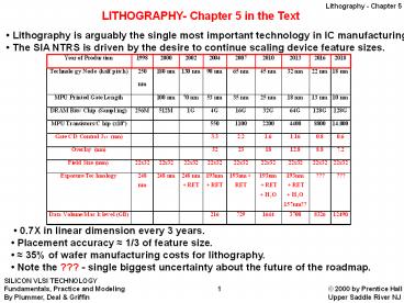
LITHOGRAPHY- Chapter 5 in the Text
Lithography is arguably the single most
important technology in IC manufacturing. The
SIA NTRS is driven by the desire to continue
scaling device feature sizes.
0.7X in linear dimension every 3 years.
Placement accuracy 1/3 of feature size. 35
of wafer manufacturing costs for lithography.
Note the ??? - single biggest uncertainty about
the future of the roadmap.
2
Historical Development and Basic Concepts
Patterning process consists of mask design,
mask fabrication and wafer printing.
It is convenient to divide the wafer
printing process into three parts A Light
source, B. Wafer exposure system, C.
Resist. Aerial image is the pattern of
optical radiation striking the top of the
resist. Latent image is the 3D replica
produced by chemical processes in the resist.
3
A. Light Sources
Decreasing feature sizes require the use of
shorter . Traditionally Hg vapor lamps have
been used which generate many spectral lines
from a high intensity plasma inside a glass lamp.
(Electrons are excited to higher energy
levels by collisions in the plasma. Photons
are emitted when the energy is released.) g
line - i line - (used for 0.5 µm,
0.35 µm) Brightest sources in deep UV are
excimer lasers
(1)
KrF - (used for 0.25 µm, 0.18µm, 0.13
µm) ArF - (used for 0.13µm, 0.09µm, . .
. ) FF - (used for ??)
Issues include finding suitable resists and
transparent optical components at these
wavelengths.
4
B. Wafer Exposure Systems
Three types of exposure systems have
been used.
Contact printing is capable of high resolution
but has unacceptable defect densities.
Proximity printing cannot easily print features
below a few µm (except for x-ray systems).
Projection printing provides high resolution and
low defect densities and dominates today.
Typical projection systems use reduction optics
(2X - 5X), step and repeat or step and scan
mechanical systems, print 50 wafers/hour and
cost 10 - 25M.
5
B1. Optics - Basics and Diffraction
Ray tracing (assuming light travels in straight
lines) works well as long as the dimensions
are large compared to . At smaller
dimensions, diffraction effects dominate.
If the aperture is on the order of , the
light spreads out after passing through the
aperture. (The smaller the aperture, the more it
spreads out.)
6
If we want to image the aperture on an
image plane (resist), we can collect the
light using a lens and focus it on the image
plane. But the finite diameter of the lens
means some information is lost (higher
spatial frequency components).
A simple example is the image formed by
a small circular aperture (Airy disk). Note
that a point image is formed only if
, or .
Diffraction is usually described in terms of
two limiting cases Fresnel diffraction - near
field. Fraunhofer diffraction - far field.
7
B2. Projection Systems (Fraunhofer Diffraction)
These are the dominant systems in use today.
Performance is usually described in terms of
resolution depth of focus field of
view modulation transfer function alignment
accuracy throughput
Consider this basic optical projection
system. Rayleigh suggested that a reasonable
criterion for resolution is that the central
maximum of each point source lie at the first
minimum of the Airy pattern. With this
definition,
(2)
(3)
The numerical aperture of the lens is by
definition, NA represents the ability of the
lens to collect diffracted light.
8
(4)
k1 is an experimental parameter which depends
on the lithography system and resist
properties ( 0.4 - 0.8). Obviously
resolution can be increased by decreasing k1
decreasing increasing NA (bigger
lenses) However, higher NA lenses also
decrease the depth of focus. (See text for
derivation.)
(5)
k2 is usually experimentally determined.
Thus a 248nm (KrF) exposure system with a NA
0.6 would have a resolution of 0.3 µm (k1
0.75) and a DOF of 0.35 µm (k2 0.5).
9
Another useful concept is the modulation
transfer function or MTF, defined as shown
below.
(6)
Note that MTF will be a function of feature
size (see text).
10
Finally, another basic concept is the
spatial coherence of the light source.
Practical light sources are not point
sources. the light striking the mask will not
be plane waves.
The spatial coherence of the system is
defined as
(7)
or often as
(8)
Typically, S 0.5 to 0.7 in modern systems.
11
B3. Contact and Proximity Systems (Fresnel
Diffraction)
Contact printing systems operate in the near
field or Fresnel diffraction regime. There is
always some gap g between the mask and resist.
The aerial image can be constructed by
imagining point sources within the aperture,
each radiating spherical waves (Huygens
wavelets). Interference effects and
diffraction result in ringing and spreading
outside the aperture.
12
Fresnel diffraction applies when
(9)
Within this range, the minimum resolvable
feature size is
(10)
Thus if g 10 µm and an i-line light source is
used, Wmin 2 µm. Summary of wafer printing
systems
13
C. Photoresists
Resists are organic polymers that are spun onto
wafers and prebaked to produce a film 0.5 -
1 µm thick.
g-Line and i-Line Resists
Generally consist of 3 components Inactive
resin Photoactive compound (PAC) Solvent -
used to adjust viscosity After spinning and
baking resists 11 PAC and resin.
Diazonaphthoquinone or DNQ resists are commonly
used today for g-line and i-line resists.
The base resin is novolac a long chain polymer
consisting of hydrocarbon rings with 2 methyl
groups and 1 OH group attached.
14
The PACs in DNQ resists are often
diazoquinones. The photoactive portion is
above the SO2. Diazoquinones are insoluble
in typical developers and reduce the
dissolution rate of unexposed resists to 1
- 2 nm sec-1.
After exposure to light, the PAC component
in DNQ resists undergoes a transformation
(Wolff rearrangement) into carboxylic acid
which is soluble in the developer (basic
solution).
15
DUV Resists
g-line and i-line resists have maximum quantum
efficiencies lt 1 and are typically 0.3.
Chemical amplification can improve this
substantially. DUV resists all use this
principle. A catalyst is used. Photo-acid
generator (PAG) is converted to an acid by photon
exposure. Later, in a post exposure bake, the
acid molecule reacts with a blocking molecule
on a polymer chain, making it soluble in
developer AND REGENERATING THE ACID
MOLECULE ? catalytic action ? sensitivity is
enhanced.
16
Basic Properties of Resists
Two basic parameters are used to describe
resist properties, contrast and the critical
modulation transfer function or CMTF.
Contrast is defined as
(11)
Typical g-line and i-line resists achieve
values of 2 - 3 and Df values of about 100 mJ
cm-2. DUV resists have much higher values (5 -
10) and Df values of about 20 - 40 mJ cm-2.
17
The aerial image and the resist contrast in
combination, result in the quality of the
latent image produced. (Gray area is partially
exposed area which determines the resist
edge sharpness.) By analogy to the MTF defined
earlier for optical systems, the CMTF for resists
is defined as
(12)
Typical CMTF values for g and i-line resists
are about 0.4. Chemically amplified DUV
resists achieve CMTF values of 0.1 - 0.2. Lower
values are better since in general CMTF lt MTF is
required for the resist to resolve the aerial
image.
18
There are often a number of additional issues
that arise in exposing resist.
- Resist is applied as a liquid and hence "flows"
to fill in the topography. - Resist thickness may vary across the wafer. This
can lead to under or over - exposure in some regions and hence linewidth
variations.
19
Reflective surfaces below the resist can
set up reflections and standing waves and
degrade resolution. In some cases an
antireflective coating (ARC) can help to
minimize these effects. Baking the resist
after exposure, but before development
can also help.
(Photo courtesy of A. Vladar and P. Rissman,
Hewlett Packard.)
20
Typical resist process
(Smaller dose for DUV resists)
(Required for DUV resists)
(g and i-line resist parameters)
21
SubWavelength Lithography
(From Synopsis Website - www.synopsis.com)
Beginning in 1998, chip manufacturers began
to manufacture chips with feature sizes
smaller than the wavelength of the light used to
expose photoresist. This is possible because of
the use of a variety of tricks - illumination
system optimization, optical pattern
correction (OPC) and phase shift mask techniques.
22
D. Illumination System Engineering
Advanced optical systems using Kohler
illumination and/or off axis illumination are
commonly used today.
Kohler illumination systems focus the
light at the entrance pupil of the objective
lens. This captures diffracted light
equally well from all positions on the mask.
Off-axis illumination also allows some of
the higher order diffracted light to be
captured and hence can improve resolution.
23
E. Mask Engineering - OPC and Phase Shifting
Optical Proximity Correction (OPC) can be used
to compensate somewhat for diffraction
effects. Sharp features are lost because
higher spatial frequencies are lost due to
diffraction. These effects can be calculated and
? can be compensated for.
From R. Socha, ASML, SPIE Microlithography Conf.
2004
24
Another approach uses phase shifting to
sharpen printed images.
A number of companies now provide OPC and
phase shifting software services. The advanced
masks which these make possible allow sharper
resist images and/or smaller feature sizes
for a given exposure system.
25
(From Rieger et. al. Layout Design . . . DAC
2001 Conf.)
Creating phase shift masks involves massive
numerical calculations and often the
implementation involves two exposures - a binary
mask and a phase shift mask - before the
resist pattern is developed.
26
Models and Simulation
Lithography simulation relies on models from
two fields of science Optics to model the
formation of the aerial image. Chemistry to
model the formation of the latent image in the
resist.
A. Wafer Exposure System Models
There are several commercially available
simulation tools that calculate the aerial
image - PROLITH, DEPICT, ATHENA. All use similar
physical models. We will consider only
projection systems. Light travels as an
electromagnetic wave.
(13)
or, in complex exponential notation,
(14)
27
Consider a generic projection system
The mask is considered to have a digital
transmission function After the light is
diffracted, it is described by the Fraunhofer
diffraction integral where fx and fy are
the spatial frequencies of the diffraction
pattern, defined as
(15)
(16)
28
?(x,y) is the Fourier transform of the mask
pattern.
(17)
The light intensity is simply the square of the
magnitude of the ? field, so that
(18)
Example - consider a long rectangular slit.
The Fourier transform of t(x) is in standard
texts and is the sin(x)/x function.
29
But only a portion of the light is collected.
This is characterized by a pupil function
(19)
The objective lens now performs the inverse
Fourier transform.
(20)
resulting in a light intensity at the resist
surface (aerial image) given by
(21)
Summary Lithography simulators perform these
calculations, given a mask design and the
characteristics of an optical system. These
simulators are quite powerful today. Math is
well understood and fast algorithms have been
implemented in commercial tools. These
simulators are widely used.
30
ATHENA simulator (Silvaco). Colors correspond
to optical intensity in the aerial image.
Exposure system NA 0.43, partially coherent
g-line illumination (? 436 nm). No
aberrations or defocusing. Minimum feature
size is 1 µm.
Same example except that the illumination
wavelength has now been changed to i-line
illumination (? 365 nm) and the NA has been
increased to 0.5. Note the improved image.
Same example except that the feature size has
been reduced to 0.5 µm. Note the poorer image.
31
B. Optical Intensity Pattern in the Resist
(Latent Image)
The second step in lithography simulation
is the calculation of the latent image in the
resist. The light intensity during
exposure in the resist is a function of time
and position because of Light absorption
and bleaching. Defocusing. Standing
waves.
These are generally accounted for by modifying
Eqn. (21) as follows
(22)
where Ir(x,y,z) models these effects (see text).
32
Example of calculation of light intensity
distribution in a photoresist layer during
exposure using the ATHENA simulator. A simple
structure is defined with a photoresist layer
covering a silicon substrate which has two
flat regions and a sloped sidewall. The
simulation shows the PAC calculated
concentration after an exposure of 200 mJ
cm-2. Lower PAC values correspond to more
exposure. The color contours thus correspond
to the integrated light intensity from the
exposure.
C. Photoresist Exposure
Neglecting standing wave effects (for the
moment), the light intensity in the resist
falls off as
(23
(The probability of absorption is proportional to
the light intensity and the absorption
coefficient.)
33
The absorption coefficient depends on the
resist properties and on the PAC (see text).
(24)
where A and B are resist parameters (first two
Dill parameters) and
(25)
m is a function of time and is given by
(26)
Substituting (24) into (23), we have
(27)
Eqns. (26) and (27) are coupled equations which
are solved simultaneously by resist
simulators.
34
The Dill resist parameters (A, B and C) can be
experimentally measured for a resist.
By measuring T0 and T8, A, B and C can be
extracted.
35
D. Photoresist Baking
A post exposure bake is sometimes used prior to
developing the resist pattern. This allows
limited diffusion of the exposed PAC and smoothes
out standing wave patterns. Generally this
is modeled as a simple diffusion process (see
text).
Simulation on right after a post exposure bake
of 45 minutes at 115 C. The color contours
again correspond to the PAC after exposure.
Note that the standing wave effects apparent
earlier have been smeared out by this bake,
producing a more uniform PAC distribution.
36
E. Photoresist Developing
A number of models for resist developing have
been proposed and implemented in lithography
simulators. The simplest is purely empirical
(Dill et.al).
(28)
where R is the local developing rate and m is the
local PAC after exposure. E1, E2 and E3 are
empirical constants.
A more physically based model has been
developed by Mack which models developer
diffusion and reaction (much like the
deposition models discussed in Chpt. 9).
See the text for details on this development
model.
37
Example of the calculation of a developed
photoresist layer using the ATHENA simulator.
The resist was exposed with a dose of 200 mJ
cm-2, a post exposure bake of 45 min at 115 C
was used and the pattern was developed for a
time of 60 seconds, all normal parameters.
The Dill development model was used. Center -
part way through development. Right - complete
development.
38
Future Trends
Optical lithography will be extendible to the
65 nm generation (maybe further - see
below). Beyond that, there is no general
agreement on which approach to use.
Possibilities include e-beam, e-beam projection
(SCALPEL), x-ray and EUV. New resists will
likely be required for these systems.
From R. Socha, ASML, SPIE Microlithography Conf.
2004
39
Summary of Key Ideas
Lithography is the key pacing item for
developing new technology generations.
Exposure tools today generally use projection
optics with diffraction limited
performance. g and i-line resists based on DNQ
materials and were used down to 0.35 µm. DUV
resists use chemical amplification and are
generally used below 0.35 µm. Lithography
simulation tools are based on Fourier optics and
do an excellent job of simulating optical
system performance. Thus aerial images can be
accurately calculated. Photoresist
modeling (exposure, development, postbake) is
less advanced because chemistry is involved
which is not as well understood. Thus latent
images are less accurately calculated today. A
new approach to lithography may be required in
the next 10 years.
Recommended
CrystalGraphics Presentations


