
Semiconductor Memory - PowerPoint PPT Presentation
1 / 36
Title:
Semiconductor Memory
Description:
When the WL rises, the capacitor CS is either charged (write 1) or discharged (write 0) ... Coupling capacitance CWBL between WL and BL causes charge ... – PowerPoint PPT presentation
Number of Views:139
Avg rating:3.0/5.0
Title: Semiconductor Memory
1
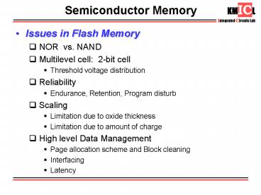
Semiconductor Memory
- Issues in Flash Memory
- NOR vs. NAND
- Multilevel cell 2-bit cell
- Threshold voltage distribution
- Reliability
- Endurance, Retention, Program disturb
- Scaling
- Limitation due to oxide thickness
- Limitation due to amount of charge
- High level Data Management
- Page allocation scheme and Block cleaning
- Interfacing
- Latency
2
Semiconductor Memory
- Non-Volatile Memory Comparison
Source Rabaey
3
Semiconductor Memory
- Random Access Memory (volatile)
- STATIC (SRAM)
- Data stored as long as supply is applied
- Large (6 transistors/cell)
- Fast
- Differential signaling
- DYNAMIC (DRAM)
- Periodic refresh required
- Small (1-3 transistors/cell)
- Slower
- Single ended signaling
4
Semiconductor Memory
- SRAM
64Kb SRAM array
5
Semiconductor Memory
- SRAM differential signaling
- Symmetrical data path to obtain reliable
operation at full speed
6
Semiconductor Memory
- 6-transistor CMOS SRAM Cell
VDD
M6
M5
Q
Q
M1
M2
GND
WL
M3
M4
BL
BL
Source Rabaey
7
Semiconductor Memory
- SRAM Read
- Precharge both bitlines high
- Then turn on wordline
- One of the two bitlines will be pulled down by
the cell - Ex q 0, qb 1, bit discharges, bit_b stays
high while q and qb bump slightly - Read stability Conditions
- q must not flip
- M1 gtgt M3 (typically 3-4 times)
8
Semiconductor Memory
- SRAM Write
- Drive one bitline high, the other low
- Then turn on wordline
- Bitlines overpower cell with new value
- Ex q 0, qb 1, bit 1, bit_b 0
- Force qb low, then q rises high
- Writability Conditions
- Must overpower feedback inverter
- M4 gtgt M6 (typically 1.5 times)
9
Semiconductor Memory
- Resistance-load SRAM Cell
WL
V
DD
R
R
L
L
Q
Q
M
M
3
4
BL
BL
M
M
1
2
10
Semiconductor Memory
- Resistance-load SRAM Cell
- Replace PMOS with resistors
- Undoped polysilicon can make T?/sq
- Reduce static power dissipation
- Need only IR gt 10-13 A to compensate leakage
current - Reduce wiring and contacts
- Reduce size by one-third
- PMOS Thin-Film Transistor SRAM Cell
- Increase cell reliability
- Less sensitivity to leakage and soft error
- Lower standby current than resistive load
11
Semiconductor Memory
- DRAM
- Invented by IBM researcher (1T) but first
marketed by Intel (3T) - Store binary data as charge on capacitance
- In contrast to the SRAM, no constraints exist on
the device size ratio - In 1T cell read process is destructive thus
stored data must be regenerated every time they
are read - Due to charge leakage, stored data need
periodically refresh - Many variations in the realization, depending on
the number of polysilicon layers, method of
capacitor formation, conductors used for row and
column
12
Semiconductor Memory
- 1T DRAM
Source Rabaey
13
Semiconductor Memory
- DRAM Write 1/0
- Data value is placed on BL (1/0)
- When the WL rises, the capacitor CS is either
charged (write 1) or discharged (write 0)
Source Rabaey
14
Semiconductor Memory
- DRAM Read 1
- Capacitor CS stored 1, Vx VBIT , BL is first
precharged to Vdd/2 VPRE - WL rises, CS shares its charge with CBL
- BL voltage increases to VBL
Source Rabaey
15
Semiconductor Memory
- Typical bit line voltage during the readout
Source Rabaey
16
Semiconductor Memory
- DRAM Read 1
- ?V change in BL will be amplify to Vdd by sense
amplifier - CBL 10 CS typical CS 30fF, ?V 200 mV
- During the readout output of sense amp is
imposed onto the bit line to restore the charge - Read and Refresh are intrinsically intertwined
17
Semiconductor Memory
- DRAM with Trench Capacitor
- Capacitance value 20 30 fF
Source Harris
18
Semiconductor Memory
- DRAM with Stack Capacitor
- Two additional Poly-Si
- are deposited above
- the transistor with a
- dielectric material
- sandwiched between
- them
- Capacitance value 20 - 30 fF in 0.35µm
- CBL 200 - 300fF
Source Hodges
19
Semiconductor Memory
- Periphery
- Decoders
- Sense Amplifiers
- Input/Output Buffers
- Control / Timing Circuitry
Source Rabaey
20
Semiconductor Memory
- Hierarchical Decoders
- Multi-stage implementation improves performance
- Structure of two-level decoder for
6-bit address
Source Hodges
21
Semiconductor Memory
- Dynamic Decoders
Precharge devices
GND
GND
WL
3
WL
3
WL
2
WL
2
WL
1
WL
1
WL
0
WL
0
V
A
A
A
A
f
DD
0
0
1
1
A
A
A
A
f
0
0
1
1
2-input NAND decoder
2-input NOR decoder
Source Rabaey
22
Semiconductor Memory
- Column Decoder
BL
BL
BL
BL
0
1
2
3
A
0
A
0
2-input NOR decoder
A
1
A
1
D
tree based
pass-transistor based
Source Rabaey
23
Semiconductor Memory
- Differential Sense Amplifier
V
DD
M
M
4
3
y
Out
M
M
bit
bit
1
2
M
SE
5
Directly applicable toSRAMs
Source Rabaey
24
Semiconductor Memory
- Differential Sensing -SRAM
V
V
DD
DD
PC
BL
BL
V
V
DD
DD
EQ
M
M
3
4
y
y
WL
i
M
M
1
2
x
x
x
x
M
SE
SE
5
SE
SRAM cell
i
V
DD
Diff.
x
x
Sense
Output
y
Amp
SE
Output
(a) SRAM sensing scheme
(b) two stage differential amplifier
Source Rabaey
25
Semiconductor Memory
- Latch-Based Sense Amplifier -DRAM
EQ
BL
BL
V
- Initialized in its meta-stable point with EQ
DD
SE
- Once adequate voltage gap created, sense amp
enabled with SE
- Positive feedback quickly forces output to a
stable operating point.
SE
Source Rabaey
26
Semiconductor Memory
- Issues in volatile memory
- SRAM and DRAM are operate under low
signal-to-noise conditions - Supply voltage reduction
- Capacitance reduction
- Increased integration density raises the noise
level due to inter-signal coupling (capacitive
crosstalk) - Wordline-to-bitline coupling
- Bitline-to-bitline coupling
- High-speed requirement increases switching noises
- Soft error more pronouncing
27
Semiconductor Memory
- Noise Sources in 1T DRAM
substrate
BL
Adjacent BL
C
WBL
-particles
WL
leakage
C
S
electrode
C
cross
28
Semiconductor Memory
- WL-BL Coupling (DRAM)
- Review capacitive crosstalk
- Coupling capacitance CWBL between WL and BL
causes charge-redistribution
29
Semiconductor Memory
- Solution open bit line architecture
- Memory array is divided in to two halves,
differential amp placed in the middle. On each
side dummy cells is added.
EQ
L
L
L
V
R
R
L
1
0
DD
0
1
SE
BLL
BLR
C
C
C
C
C
C
S
S
S
SE
S
S
S
Dummy cell
Dummy cell
Source Rabaey
30
Semiconductor Memory
- Leakage
- Sub-threshold current to BL more serious due to
low Vth - Tunneling leakage current more serious due to
thin oxide - pn junction leakage is small since cell is small
- Leakage current across field oxide. Trench
isolation can help
BL
BL1
WL
Itunnel
Ijunc
Isub
Icell-to-cell
31
Semiconductor Memory
- Data Retention Dissipation
- SRAM
- Increasing Vth using body biasing
- Inserting extra resistance in the leakage path
- Lowering supply voltage
- DRAM
- Dynamically controlled Vth well biasing access
transitor - Turn off device hard apply a negative voltage
on WL - Raise bit line voltage of unused cells
32
Semiconductor Memory
- Density Improvement
- Deep sub-micron feature size
- Stacked capacitor in DRAM
- High dielectric constant material such as BST
- SOI-DRAM results in better isolation (Z-RAM)
- Various Access Methods
- Fast page mode (FP)
- Extended data output (EDO)
- Synchronous DRAM (SDRAM)
- Double data rate (DDR)
- Direct Rambus DRAM (DRDRAM)
33
Semiconductor Memory
Row
Address
Redundant
rows
Fuse
Bank
Redundant
columns
Memory
Array
Column
Column Decoder
Address
Redundancy in memory array increases the yield.
Source Jan Rabaey
34
Semiconductor Memory
- SRAM vs. DRAM
Source S. Natarajan, et al, IEEE Solid-State
Circuits Magazine v1 no3 2009
35
Semiconductor Memory
- Embedded SRAM vs. DRAM Scaling Trend
- Embedded DRAM is three to five times denser in
the same technology
Source S. Natarajan, et al, IEEE Solid-State
Circuits Magazine v1 no3 2009
36
Semiconductor Memory
- Embedded SRAM vs. DRAM
- Standby current increases as device gets smaller
Source S. Natarajan, et al, IEEE Solid-State
Circuits Magazine v1 no3 2009
Recommended
CrystalGraphics Presentations


