
LNA Schematic - PowerPoint PPT Presentation
1 / 9
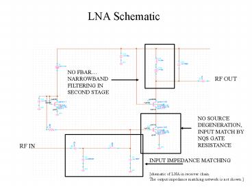
Title: LNA Schematic
1
LNA Schematic
NO FBAR NARROWBAND FILTERING IN SECOND STAGE
RF OUT
NO SOURCE DEGENERATION, INPUT MATCH BY NQS GATE
RESISTANCE
RF IN
INPUT IMPEDANCE MATCHING
shematic of LNA in receiver chain. The output
impedance matching network is not shown.
2
Chip Photo
Testing is currently in progress
3
Inductor Modeling
- Convert measured S parameters to circuit model.
Method for de-embedding S Parameters
4
Pi Circuit Model
L 9.8 nH Rs 5 ohm Cp1, Cp2 250 fF Rp1, Rp2
220 ohm
5
Inductor S Parameters
6
Next Generation LNA
- Reuse bias current by stacking second stage on
top of first one. - Signal coupled from first stage to second.
- Bypass capacitor allows for two amplifying
stages.
7
Optimizing Gm
Need to consider input parasitic capacitance Cp,
which comes from bonding pads and ESD protection
diodes
8
Optimization Plots
- Gm and NF plots for varying device width
9
Simulations
42 dB
1 dB