
Analog to Digital Converters - PowerPoint PPT Presentation
Title:
Analog to Digital Converters
Description:
One conversion every clock period. Cons. Matching errors digital correction for n 8 ... Histogram test provides information on each code transition. ... – PowerPoint PPT presentation
Number of Views:273
Avg rating:3.0/5.0
Title: Analog to Digital Converters
1
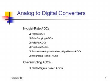
Analog to Digital Converters
- Nyquist-Rate ADCs
- Flash ADCs
- Sub-Ranging ADCs
- Folding ADCs
- Pipelined ADCs
- Successive Approximation (Algorithmic) ADCs
- Integrating (serial) ADCs
- Oversampling ADCs
- Delta-Sigma based ADCs
2
Conversion Principles
3
ADC Architectures
- Flash ADCs High speed, but large area and high
power dissipation. Suitable for low-medium
resolution (6-10 bit). - Sub-Ranging ADCs Require exponentially fewer
comparators than Flash ADCs. Hence, they consume
less silicon area and less power. - Pipelined ADCs Medium-high resolution with good
speed. The trade-offs are latency and power. - Successive Approximation ADCs Moderate speed
with medium-high resolution (8-14 bit). Compact
implementation. - Integrating ADCs or Ramp ADCs Low speed but
high resolution. Simple circuitry. - Delta-Sigma based ADCs Moderate bandwidth due
to oversampling, but very high resolution thanks
to oversampling and noise shaping.
4
Performance Limitations 1
Thermal Noise Limitation
Clock Jitter (Aperture) Limitation
Normalized Noise Powers
fin½fconv
Limiting Condition
Maximum Resolution
5
Performance Limitations 2
Displays
Seismology
Audio Sonar
Wireless Communications
Ultra Sound
Video
? Selection of ADC Architecture is driven by
Application
6
Parallel or Flash ADCs
Conceptual Circuit
7
Sub-Ranging ADCs
Half-Flash or Two-Step ADC
8
Folding ADCs
Principle Configuration
9
Folding Processor
Example 2-Bit Folding Circuit
(2n-11)Io for n-Bit
2Io
10
Successive Approx. ADCs
Implementation
Concept
11
DAC Realization 1
(Voltage Mode)
12
DAC Realization 2
Spread Reduction through R-2R Ladder
13
DAC Realization 3
Charge-Redistribution Circuit
valid only during f2
- Pros
- Insensitive w.r.t. Op-amp Gain
- Offset (1/f Noise) compensated
- Cons
- Requires non-overlapping Clock
- High Element Spread ? Area
- Output requires SH
14
DAC Realization 4
Spread Reduction through capacitive Voltage
Division
Example 8-Bit ADC
valid only during f2
Spread2n/2
15
DAC Realization 5
Charge-Redistribution Circuit with Unity-Gain
Amplifier
Example 8-Bit ADC
Amplifier Input Cap.
16/15C
Spread½2n/2
Cp ? Gain Error ?G-Cp/16C
- Pros
- Voltage divider reduces spread
- Buffer ? low output impedance
- No clock required
- Cons
- Parasitic cap causes gain error
- High Op-amp common mode input required
- No amplifier offset compensation
16
DAC8 with Unity-Gain Amplifier
17
DAC Realization 6
Current Mode Implementation
18
Current Cell Floor Plan
Symmetrical Current Cell Placement
Array of 256 Cells
Current summing Rail
Iout
Unit Current Cell
R
Switching Devices
Cascode Current Source
19
DAC Implementation
Layout of 10-Bit Current-Mode DAC (0.5mm CMOS)
Current summing Rails
20
Modified SA Algorithm 1
Idea Replace DAC by an Accumulator ?
Consecutively divide Ref by 2
21
Modified SA Algorithm 2
Idea Maintain Comparator Reference (½ FSGnd)
? Double previous Accumulator Output
First cycle only
Accumulator
22
SC Implementation
SC Implementation of modified SA ADC
23
Timing Diagram
24
Offset Compensated Circuit
Offset Compensated SC Implementation
25
Building Blocks 1
Transconductance Amplifier
DC Gain 77 dB
Gain-bandwidth 104 MHz _at_ CL 1.5 pF
Power 1.3 mW
Output Swing 4 V p-p
26
Building Blocks 2
Latched CMOS Comparator
Power 0.5 mW
Resolution gt 0.5 mV
Settling Time 3 ns
27
Layout of 8-Bit ADC
165 mm (0.5 mm CMOS)
28
Spice Simulation (Bsim3)
8-Bit ADC fclk10MHz ? fconv1.25MHz
29
Pipelined ADCs
Pipelined modified SA or Algorithmic ADC
- Pros
- Offset (1/f Noise) compensated
- Minimum C-spread
- One conversion every clock period
- Cons
- Matching errors ? digital correction for ngt8
- Clock feed-through very critical
- High amplifier slew rate required
30
Integrating or Serial ADCs
Dual Slope ADC Concept
Constant Ramp
Prop. to Input Ramp
- Using 2N/k samples requires Ref FS/k
- reduced Integrator Constant
- (Element Spread)
N represents digital equivalent of analog
Input
31
SC Dual-Slope ADC
10-Bit Dual-Slope ADC
32
ADC Testing
- Types of Tests
- Static Testing
- Dynamic Testing
- In static testing, the input varies slowly to
reveal the actual code transitions. ? Yields INL,
DNL, Gain and Offset Error. - Dynamic testing shows the response of the
circuit to rapidly changing signals. This reveals
settling errors and other dynamic effects such as
inter-modulation products, clock-feed-trough,
etc.
33
Performance Metrics 1
Static Errors
IDEAL ADC
- Error Types
- Offset
- Gain
- DNL
- INL
- Missing Codes
34
Performance Metrics 2
Frequency Domain Characterization
Ideal n-Bit ADC SNR 6.02 x n 1.76 dB
35
ADC Error Sources
- Static Errors
- Element or Ratio Mismatches
- Finite Op-amp Gain
- Op-amp Comparator Offsets
- Deviations of Reference
- Dynamic Errors
- Finite (Amplifier) Bandwidth
- Op-amp Comparator Slew Rate
- Clock Feed-through
- Noise (Resistors, Op-amps, switched Capacitors)
- Intermodulation Products (Signal and Clock)
36
Static Testing
- Servo-loop Technique
- Comparator, integrator, and ADC under test are
in negative feedback loop to determine the analog
signal level required for every digital code
transition. - Integrator output represents equivalent analog
value of digital output. - Transition values are used to generate
input/output characteristic of ADC, which reveals
static errors like Offset, Gain, DNL and INL.
37
Dynamic Testing
Test Set-up
- Types of Dynamic Tests
- Histogram or Code-Density Test
- FFT Test
- Sine Fitting Test
38
Histogram or Code-Density Test
- DNL appears as deviation of bin height from
ideal value. - Integral nonlinearity (INL) is cumulative sum
(integral) of DNL. - Offset is manifested by a horizontal shift of
curve. - Gain error shows as horizontal compression or
decompression of curve.
39
Histogram Test
- Pros and Cons of Histogram Test
- Histogram test provides information on each code
transition. - DNL errors may be concealed due to random noise
in circuit. - Input frequency must be selected carefully to
avoid missing codes (fclk/fin must be
non-integer ratio). - Input Swing is critical (cover full range)
- Requires a large number of conversions (o 2n x
1,000).
40
Simulated Histogram Test
8-Bit SA ADC with 0.5 Ratio Error and 5mV/V
Comparator Offset
41
FFT Test
- Pros and Cons of FFT Test
- Offers quantitative Information on output Noise,
Signal-to-Noise Ratio (SNR), Spurious Free
Dynamic Range (SFDR) and Harmonic Distortion
(SNDR). - FFT test requires fewer conversions than
histogram test. - Complete characterization requires multiple
tests with various input frequencies. - Does not reveal actual code conversions
42
Simulated FFT Test
8-Bit SA ADC with 0.5 Ratio Error and 5mV/V
Comparator Offset
SNDR49 dB
? ENOB7.85
SFDR60 dB