
Bipolar Junction Transistors: Basics - PowerPoint PPT Presentation
1 / 35
Title:
Bipolar Junction Transistors: Basics
Description:
Measure of hole current vs total emitter current. Electron 'backwards' current detracts from ... The SiO2 is etched and an arsenic implant forms the N regions. ... – PowerPoint PPT presentation
Number of Views:135
Avg rating:3.0/5.0
Title: Bipolar Junction Transistors: Basics
1
Bipolar Junction Transistors Basics
2
BJT Symbols and Currents
3
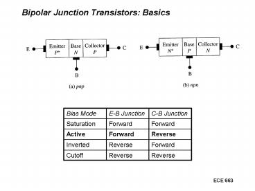
BJT configurations
4
BJT Fabrication
5
PNP BJT Electrostatics
6
NPN Transistor Band Diagram Equilibrium
7
PNP Transistor Active Bias Mode
8
PNP Physical Currents
9
PNP transistor amplifier action
10
Emitter Injection Efficiency - PNP
- Measure of hole current vs total emitter current
- Electron backwards current detracts from
amplification - Want ? as close as possible to 1 for high gain
11
Base Transport Factor - PNP
- How many of the holes injected into the base make
it to the other side? - Again,
- Want ?T as close as possible to 1 for high gain
- Recombining holes dont help
12
Common Base DC current gain - PNP
- Common Base Active Bias mode
13
Common Base DC current gain - PNP
14
Common Emitter DC current gain - PNP
IC
IB
IE
15
PNP BJT Common Emitter Characteristic
16
Supplementary Material Bipolar Transistor
Flow Junction Isolation Process
17
Following initial cleaning, an SiO2 layer is
thermally grown on the silicon substrate.
Photoresist is spun on the wafer to prepare for
the first masking operation.
18
Mask 1 patterns the photoresist. The SiO2 layer
is removed where it is not protected by the
photoresist by dry etching.
19
An N implant is performed to dope the buried
layer region. As or Sb would typically be used
here because they have smaller diffusivities than
P.
20
The buried layer is driven in using a high
temperature furnace cycle.
21
The SiO2 is etched off the surface and an N type
epitaxial layer is grown. Note that during the
epi growth, the buried layer diffuses upwards
22
SiO2 is thermally grown on the surface and
photoresist is spun on. Mask 2 is used to define
the resist and then the SiO2 layer is etched
using the resist as a mask.
23
A boron implant dopes the isolation regions.
24
The P isolation regions are driven down to the P
substrate to laterally isolate the devices. SiO2
is grown on the surface during this drive-in.
Note that the buried layer continues to diffuse
upwards during this high temperature step.
25
Photoresist is spun onto the wafer and mask 3 is
used to define the base regions. The SiO2 is
etched and a boron implant forms the base region.
26
The base region is driven-in to its final
junction depth. A surface SiO2 layer is grown as
part of this drive-in process.
27
Photoresist is spun onto the wafer and mask 4 is
used to define the emitter and collector contact
regions. The SiO2 is etched and an arsenic
implant forms the N regions.
28
The N regions are driven-in to their final
junction depth. A surface SiO2 layer is grown as
part of this drive-in process.
29
Photoresist is spun onto the wafer and mask 5 is
used to define the contact regions. The SiO2 is
etched.
30
Aluminum is deposited on the wafer. Photoresist
is then spun onto the wafer and mask 6 is used
to define the wiring regions. The Al is then
etched. Stripping the photoresist completes the
overall process flow.
31
N
N
P
P
P
N
N
P
Diodes can be made with the metal mask connecting
the collector and base together Resistors made
with two contacts to any isolated doped area
32
Oxide-isolated bipolar process
33
Self-Aligned Double Poly Bipolar - NPN
34
(No Transcript)
35
Self-Aligned Double Poly Bipolar - NPN
Recommended
CrystalGraphics Presentations


