
APV25 for SuperBelle SVD - PowerPoint PPT Presentation
Title:
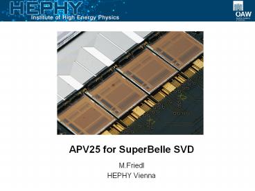
APV25 for SuperBelle SVD
Description:
Every sensor is read out individually (no ganging) ... ganged. Beam test result shows that already ganging of 2 sensors is problematic. 22 ... – PowerPoint PPT presentation
Number of Views:40
Avg rating:3.0/5.0
Title: APV25 for SuperBelle SVD
1
APV25 for SuperBelle SVD
- M.Friedl
- HEPHY Vienna
2
APV25
Schematics of one channel
- Developed for CMS by IC London and RAL (70k chips
installed) - 0.25 µm CMOS process (gt100 MRad tolerant)
- 40 MHz clock (adjustable), 128 channels, analog
pipeline - 50 ns shaping time (adjustable)
- Low noise 250 e 36 e/pF
- cf. BEETLE (LHCb) 497 e 48 e/pF
- cf. SVX4 (CDF,D0) 728 e 56 e/pF
- Multi-peak mode (read out several samples along
shaping curve)
3
APV25 Pipeline Triggers
4
APV25 Pipeline
- 192 pipeline cells (actually a ring buffer)
- After APV receives a trigger, the corresponding
pipeline cells are labelled in an index FIFO in
order not to be overwritten before the event is
completely read out - Index FIFO has 32 cells
- ? In worst case, 160 pipeline cells always
remain active - 3.8µs _at_ 42.3MHz clock (RF/12)
- ? 3.5µs max. latency for L1
- or
- 5.0µs _at_ 31.8MHz clock (RF/16)
- ? 4.7µs max. latency for L1
- Preferred by Iwasaki-san, but has implications on
trigger rate (see below)
5
APV25 Triggers
(Pipeline delay and propagation delays are not
shown in this plot)
- APV controller (NECO) generates 2 consecutive
trigger symbols (100) to APV from L1, resulting
in 6 samples along shaped waveform - ? allows peak time reconstruction (few ns
precision, see talk by C.I.) - No triggers allowed during 6 clocks after L1
6
APV25 Trigger Restrictions
- (1) Minimum L1 distance of 6 APV clocks
- (2) Maximum pipeline index FIFO filling of 32
- Lets see what (2) means
7
APV Output and FIFO Filling (1)
- Single L1 trigger resulting in 6 samples
APV25 output tick marks (idle) header 128 strip
data
8
APV Output and FIFO Filling (2)
- Two L1 triggers resulting in 12 samples
9
APV Trigger Simulation (1)
- Input CLK, L1 rate
- Model APV25 state machine, exponential trigger
distribution - Output FIFO filling histogram, trigger loss,
Poisson distribution to check randomness of
simulated triggers
Downloadhttp//belle.hephy.at/apvtrg.zip (needs
Labwindows/CVI 8.1 run-time engine from
http//ni.com)
10
APV Trigger Simulation (2)
- Min Lost trigger restriction (1) too little
distance - FIFO Lost trigger restriction (2) too many
pending readouts - Nakao-san wishes lt3 dead time _at_ L130kHz
- ? OK (0.87) for 42.4MHz clock, slightly higher
(3.43) at 31.8MHz
11
Chip-on-Sensor Concept
12
Possible SuperSVD Layout
cm
layers
5
4
3
2
1
cm
- Using 6 DSSDs (12.5 cm long, up to 4 cm wide)
- Every sensor is read out individually (no
ganging) - Edge sensors (green) are conventionally read from
side - Center sensors (red) use chip-on-sensor concept
(layers 3-5)
13
Origami Concept
- Extension of chip-on-sensor to double-sided
readout - Flex fan-out pieces wrapped to opposite side
(hence Origami) - All chips aligned on one side ? single cooling
pipe
Side View (below)
14
Origami Layout
Connectors (on both sides)
2 p-side APV chips
2 p-side APV chips
4 n-side APV chips
- 3-layer flex hybrid design done
- p- and n-sides are separated by 80V bias
- n-side pitch adapter is integrated in hybrid
- to be manufactured at CERN PCB workshop
Flex fanouts to be Wrapped around the sensor edge
15
3D Rendering
(readout connections not shown)
16
APV25 Purchase
- SuperSVD needs about 2500 normal 2500 thinned
chips (for chip-on-sensor) including spares - Enough tested APV25 chips are in stock _at_ IC
London - Purchase procedure of 4000 APV25 chips in JFY
2008 in underway - 1000 more will be purchased next year (due to
administrative limits) - 1 APV25 costs 28 CHF (18 , 2150 , 23 )
- Thinning will be taken care of by HEPHY Vienna
- Existing chips are 300µm thick, thinning target
150µm - In parallel, discussion for a readout chip
development by IDEAS has started for a future
upgrade of SuperSVD - Based on APV25 design
17
Summary Outlook
- APV25 chip (developed for CMS) fits for SuperSVD
- Pipeline length and dead time simulation _at_ 30kHz
Poisson triggers - 0.87 _at_ 42.4MHz clock, 3.8µs pipeline
- 3.43 _at_ 31.8MHz clock, 5.0µs pipeline
- Trade-off between wishes of Nakao-san and
Iwasaki-san - Origami concept for low-mass double-sided
readout with cooling - We will assemble such a module in the near future
18
BACKUP SLIDES
19
Comparison VA1TA APV25
- VA1TA (SVD2)
- Commercial product (IDEAS)
- Tp 800ns (300 ns 1000 ns)
- no pipeline
- lt10 MHz readout
- 20 Mrad radiation tolerance
- noise ENC 180 e 7.5 e/pF
- time over threshold 2000 ns
- single sample per trigger
- APV25 (SuperSVD)
- Developed for CMS by IC London and RAL
- Tp 50 ns (30 ns 200 ns)
- 192 cells analog pipeline
- 40 MHz readout
- gt100 Mrad radiation tolerance
- noise ENC 250 e 36 e/pF
- time over threshold 160 ns
- multiple samples per trigger possible
(Multi-Peak-Mode)
20
Shaping Time and Occupancy
BEAM PARTICLE
OFF-TIMEBACKGROUND PARTICLE
21
Ganged Sensors Read Out with APV25
- Prototype module with 2 partially ganged DSSDs
- Beam test result shows that already ganging of 2
sensors is problematic
ganged ganged single single
p-side n-side p-side n-side
Cluster SNR 9.4 10.1 13.1 13.9
Single Strip SNR 13.5 13.4 19.9 18.9
22
Flex_Module Measurement Results
- Beam test result shows that chip-on-sensor
(n-side) delivers excellent SNR
Flex_Module Flex_Module Conventional (single sensor) Conventional (single sensor)
p-side n-side p-side n-side
Cluster SNR 13.8 18.4 13.1 13.9
Single Strip SNR 20.9 25.4 19.9 18.9
23
Origami Material Budget
- X0 comparison between conventional and
chip-on-sensor
- 50 increase in material, but also huge
improvement in SNR - Trade-off between material budget and SNR
- According to simulation, additional material is
prohibitive in 2 innermost layers, but no problem
for layers 3-5 ? OK with layout
Recommended
CrystalGraphics Presentations


