
GigE Interface Board - PowerPoint PPT Presentation
1 / 19
Title:
GigE Interface Board
Description:
SATA is a computer bus technology primarily designed for transfer of data to and from a hard disk. ... Glue Logic will have to check the data packets from SATA ... – PowerPoint PPT presentation
Number of Views:44
Avg rating:3.0/5.0
Title: GigE Interface Board
1
GigE Interface Board
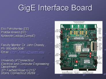
- Eric Petrichenko (EE)
- Pratiba Anand (EE)
- Kolawole Ladoja (CompE)
- Faculty Mentor Dr. John Chandy
- Ph 860-486-5047
- Email John.Chandy_at_uconn.edu University of
Connecticut - Electrical and Computer Engineering Department
- 371 Fairfield Road U-2157 Storrs, Connecticut
06269
2
Background
- Many advances in computer technology recently but
access time have not kept up - Great need for high-performance storage systems
- Therefore a storage network is being built
- Using a Benes Network
- Is a type of multistage switching network
Figure 1. Benes Network
3
Introduction
- Our project
- To create a board that fills in the hole from
SATA to GigEthernet (will be explained in more
detail later)
Figure 2. Project Outline
4
Specifications
5
SATA (Serial Advanced Technology Attachment)
- Introduction
- SATA is a computer bus technology primarily
designed for transfer of data to and from a hard
disk. - Replacement for the Parallel ATA physical storage
interface. - SATA uses a 7 wire interface. Three of the wires
are ground signals. The other 4 are two pairs of
differential signals - one pair in each
direction. - Advantages of switching to SATA from Parallel
ATA greater speed, simpler upgradeable storage
devices and easier configuration.
6
SATA-Xilinx (XUP V2-Pro)
- Only four of the available eight channels are
used on the XUP Virtex-II Pro Development System.
- Three channels are equipped with low-costs SATA
connectors and the fourth channel terminates at
user-supplied Sub-Miniature A (SMA) connectors. - The SATA channels are split into two interface
formats, two HOST ports and a TARGET port. - The SATA data rate is less than 2.5 Gb/s so the
75 MHz clocks
Figure 2. SATA Part of the Board
7
SATA-Protocol
- The SATA Frame structure used between Host and
Device is shown in the figure. - The SATA frame begins with a Start-of-frame
SOF. - The SOF is followed by the Frame Information
Structure FIS. - Then the Cyclic Redundancy Code CRC is placed
in the frame. - The final block in the message is an End-of-Frame
EOF.
Figure 3. SATA Bus Protocol Frame
8
Ethernet
- Ethernet is comprised of MAC and PHY
- Diagram below shows the flow from SATA to Ethernet
Figure 4. Detailed diagram of GigEthernet
9
What is the Media Access Control (MAC) Sub Layer?
- One of two sublayers that make up the Data Link
Layer of the OSI model - Controls how a computer on the network gains
access to the data and permission to transmit it.
Figure 5. Flow Chart of OSI.
10
MAC Sub Layer
- Acts as an interface between the Logical Link
Control sublayer and the network's physical layer
- Primarily concerned with the control of access to
the physical transmission medium.
Figure 6. IEE802 Diagram.
11
Purpose of MAC
- Moves data packets to and from one Network
Interface Card (Xilinx XUP-V2Pro) to another.
Figure 7. MAC encapsulation of a packet of data
12
Specific Chip Options
- Intel 82547EI Gigabit Ethernet Controller Intel
MAC with integrated PHY. Uses a CSA bus protocol
to get data onto the chip. Therefore an
interface between SATA and CSA would be necessary
for this chip. - PMC 3386 Does not contain an integrated PHY. To
connect with a PHY it uses the industry standard
GMII protocol. Contains dual GigE MACs which is
beneficial because each board is connected to 2
Ethernet lines. - Build MAC Our Self Use open core Gigabit MAC
and put on the FPGA along with our SATA logic.
We would then need an external PHY which also
uses the industry standard GMII protocol.
13
Glue Logic
- Purpose
- To accept the data packets from either Ethernet
or SATA and make it compatible with the other - Ethernet SATA or Vice versa
- Discrete Logic? No
- Why?
- Delay each chip has it own propagation delay.
Accumulative delay will be difficult to calculate
and may be too much. As you know, our project is
time sensitive. - Difficult to Debug - if there is an error, we
will have to check the input and outputs of each
individual chip to find it. This can be time
consuming. - Cost - individually, chips are cheap. However
with the number of chips that will be required,
the overall cost can quickly become exorbitant. - Other choice?
14
Glue Logic
- FPGA (Field Programmable Gate Array)
- Delay - Only one chip needed, so there is only
one propagation delay. - Cost there is only the initial cost of the
FPGA, nothing more. The software needed to
program the FPGA can either be gotten online or
written by the team. - Opencores.org
- Debugging easier to debug only software errors
which can be easily found using proper
programming techniques. - Piece of cake? Not Easy
15
Glue Logic
- There are three major concerns
- Data format
- Data needs to be extracted form one format and
modified into another
- Error checking
- Corrupted or invalid data is of no use to the
user. - Glue Logic will have to check the data packets
from SATA or Ethernet for errors. Also, it may
have to provide some kind of data packet
information so that SATA or the Ethernet can
check if the data packet has been corrupted of
not.
16
Glue Logic
- Data transfer Rates
- SATA Less than 2.5 GBits/s
- Ethernet steady rate of 1Gbits/s
- Clock rate of 1.25 GHz
- SATA transfers data serially while Ethernet
transfers data in parallel. - How do we plan to solve this problem? With the
use of SERDES (serializer / deserializer) and
buffers
Figure 8. Block Diagram of Glue Logic
17
Timeline
- Spring 2007
- Complete design in VHDL code
- Complete testing of the design
- Send out specs of PCB for manufacturing
- Implementing and testing the Final Product
- Fall 2006
- Preliminary design
- Implementation in VHDL code
- Ordering supplying
18
Budget
19
What we discussed today?
- Designing an GigE interface board.
- Purpose and motivation
- SATA
- MAC
- PHY
- GLUE Logic
Recommended
CrystalGraphics Presentations


