
Film Deposition in IC Fabrication - PowerPoint PPT Presentation
1 / 12
Title:
Film Deposition in IC Fabrication
Description:
Adherent. Uniformity, no pin holes. Conformal step coverage. Thermal & electrical stability ... Electron wind and field-driven atomic migration. Bamboo-structured wire ... – PowerPoint PPT presentation
Number of Views:165
Avg rating:3.0/5.0
Title: Film Deposition in IC Fabrication
1
Film Deposition in IC Fabrication
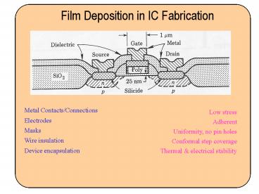
Metal Contacts/Connections Electrodes Masks Wir
e insulation Device encapsulation
Low stress Adherent Uniformity, no pin
holes Conformal step coverage Thermal
electrical stability
2
Vapor pressure of metals
3
Sputter Deposition Systems
RF Sputter System
Voltage ratio in RF sputtering VC/VA (AA/AC)n
E
DC Sputter Deposition
Magnetron Sputter Deposition
4
Chemical Vapor Deposition (CVD)
Plasma-enhanced CVD (PECVD)
Low-pressure CVD (LPCVD)
5
Different thin film textures
Single crystal
Poly-crystalline
Poly-crystalline columnar
Nano-crystalline
amorphous
6
Step Coverage of Deposited Films
High surface mobility non-directional flux ?
conformal step coverage
7
Electromigration Effects
Void Pile-up
Bamboo-structured wire
Electromigration-resistant
Electron wind and field-driven atomic migration
8
SiO2 Films for masking protection
SiH4 O2 ? SiO2 2H2 or SiH4 N2O? SiO2
2N2 2H2 by APCVD or
LPCVD at 450ºC, SiH4 diluted in H2 with
Si(C2H5O)4 (TEOS), more stable to handle
Si(C2H5O)4 12O2 ? SiO2 8CO2 10H2O, APCVD
or LPCVD at 700ºC SiO2 films by PECVD at
300-350ºC, low compressive stress. Applications
of deposited SiO2 films Field oxide for
MOS and HV devices (deposited on thermal SiO2)
Fill-in of the isolation walls/wells
Isolation between multi-layer metal connections
Diffusion and implantation masks
Final encapsulation layer
9
Other Films for masking protection
- Phosphosilicate glass (PSG)
- adding P2O5 to improve the quality of SiO2
- mixing PH3 or (CH3O)3P in oxidation gases
- 2PH3 4O2 ? P2O5 3H2O
- or 2(CH3O)3P 10O2 ? P2O5 6CO2 10H2O
- Effect of P2O5 reduce tensile stress in SiO2
(to 0 at 20 P2O5) - TCE(?) matching with
substrate (P2O5 raises ?) - improve film texture
(denser, void-free) - effective diffusion
barrier to Na - Si3N4 (and SiOxNy) more stable than SiO2,
excellent barrier - to Na, B and Ga migration, mask for
oxidation - 3SiH4 4NH3 ? Si3N4 12H2 (PNH3
PSiH4 150) - LPCVD at 900ºC, high tensile stress,
t lt 1000Å - PECVD at 300ºC, low stress, high H
incorporation - RF sputtering of Si in N2 discharge
3Si 4N ? Si3N4
10
Pit Formation of Al Contact with Si
High solubility of Si in Al (1)
Al spikes
11
Silicide Contacts
5.8
10.5 10.4 13 43 20 5.3 42
13 5.3 14.5 7
Resistivity of metal
12
Phase Diagram and Formation Sequence of Silicide
Oxidation of Silicide