
12'4 MOS Transistor Matching - PowerPoint PPT Presentation
1 / 33
Title:
12'4 MOS Transistor Matching
Description:
Consider a MOS transistor with a couple of Gate fingers. ... when Vds is large, tilted implant has strong impact on hot-carrier generation ... – PowerPoint PPT presentation
Number of Views:215
Avg rating:3.0/5.0
Title: 12'4 MOS Transistor Matching
1
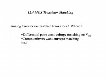
12.4 MOS Transistor Matching
- Analog Circuits use matched transistors ! Where
? - Differential pairs want voltage matching on VGS
- Current mirrors want current matching
- etc.
2
- Differential pair Consider M1 and M2 biased
at the same current, but have a voltage mismatch - of DVGS. For input signal Vin, then
- V1 VGS Vin/2 and
- V2 VGS DVGS Vin/2.
- V2 V1 DVGS Vin.
- Therefore, a DC offset voltage of DVGS.
Current mirror Consider M1 (which is diode
connected) and M2 biased at the same VGS.
Here, I1 IREF ½ k1 (W/L)1 VGSt12, and
I2 ½ k2 (W/L)2 VGSt22. If the
transistors are well matched, then k1
k2 Vt1 Vt2 ? VGSt1 VGSt2 Well matched
case I2/IREF (W/L)2/(W/L)1 1 (suppose). IF,
however, transistors are mismatched, then k and
Vt are mismatched for M1 and M2. This leads to
I2 IREF DI (Current mismatch).
3
12.4 MOS Transistor Matching
MOS transistors can be optimized either for
voltage matching or for current matching, but
not for both !
gt Why ?
4
- (1)Voltage matching
- Suppose two transistors, M1 and M2, operate at
equal drain currents. - Then, the possible voltage mismatch
- OFFSET Voltage DVGS DVt Vgst (Dk/2k2)
- To minimize DVGS
- use large W/L and low operating currents.
- minimize Vgst Vgst 0.1 volts or less.
5
(2) Current matching The mismatch between ID1
and ID2 ID2/ID1 k2/k1 (1 2DVt/Vgst) DId
/ Id Dk/k 2DVt/Vgst ? To optimize ? use
reasonably large Vgst Vgst 0.3 V or more !
6
So, Vgst 0.1 V or less for voltage matching and
Vgst 0.3 V or more for current
matching. Next is the effect of geometric
factors on the matching !
7
- Geometric Effects on Matching.
- Increased Gate Area minimizes impact of local
fluctuations ? Large transistors match more
precisely. - Longer channels reduce line width variations and
channel length modulation ? Long-channel
transistors match more precisely. - Orientation of MOSFET matters.
- ? Gate Area, Oxide thickness, Channel length
modulation, Orientation,
8
- (1)Gate Area
- Vt mismatch SVt standard deviation
- SVt CVt / (Weff Leff)1/2
- Where CVt constant.
- Only applies to carefully laid out MOS for
optimal matching. - Leff, Weff ? Ld, Wd if they are several times
greater than minimum.
9
- (1)Gate Area
- k-mismatch Sk standard deviation in device
transconductance. - Sk / k Ck / (Weff Leff)1/2
- Where Ck constant.
- Linewidth variation
- Gate oxide roughness
- Statistical variation in mobility
Edge effect when L lt 2um, then peripheral
variations affect k. Sk/k ( C2k/WeffLeff
C2kp1/W2effLeff C2kp2/WeffL2eff)1/2
10
(2)Gate Oxide Thickness Scaling down to thinner
oxide ? seems to improve Vt-matching. ? not
affected is k-matching.
CVt a tox Nb1/2
11
- (3)Channel-length Modulation
- Short-channel MOSFETs ? severe mismatch in L if
different VDS ! - Mismatch DVDS / L
- Notes
- Ld 15-25 mm, adequate for noncritical use such
as current distribution network. - Operate matched transistors at equal VDS by
e.g., Cascoding.
12
- (4) Orientation
- Several mismatch error
- Si wafer is under stress due to processing.
- The stress produces anisotropic effect on the
carrier mobility, etc. - Different orientation ? different stress effect
on the transconductance
- Stress-induced mobility variation ? several
current mismatch - For example, tilted wafer ? as much as 5 in
current matching errors.
13
(4) Orientation
- Layout Editing
- Be careful with Cell editing when the matched
transistors belong in different cells ! - Group matched devices into the same cell
- May be more difficult to understand in the
Schematics - But safer for the matching !
14
(4) Orientation
15
(4) Orientation
- Mirror-image layout vs. Superimposable layout
- Mask misalignment ? same effect on
superimposable but opposite effect on
mirror-image. - So, be careful on asymmetric devices such as
Extended Drain MOS.
16
- Diffusion and Etch effects on Matching
- (1) Effects of Poly Gate etching
- Consider the mask-step of defining Poly Gates
- Deposit Poly ? cover with oxide ? Mask pattern
for opening in oxide ? remove Poly in open
region by etching - Etch rate depends on the size of Opening
- Larger opening ? faster etch.
17
- Diffusion and Etch effects on Matching
- (1) Effects of Poly Gate etching
- Consider the mask-step of defining Poly Gates
- Deposit Poly ? cover with oxide ? Mask pattern
for opening ?
remove Poly open region by etching - Etch rate depends on the size of Opening
- Larger opening ? faster etch.
18
Diffusion and Etch effects on Matching
- Dummy Gates need be electrically connected to
prevent spurious signal. - Best to connect Dummy Gates to the Backgate.
19
- (3)Contacts over the Gate Poly
- Contacts in the active Gate region ? gross
variations in Vt ! - Gate contacts must be outside the active region,
on thick field-oxide. - Probably because of grain size, work function,
dopants, stress,
20
- (3)Contacts over the Gate Poly
- Contacts in the active Gate region ? gross
variations in Vt ! - Gate contacts must be outside the active region,
on thick field-oxide. - Probably because of grain size, work function,
dopants, stress, - Annular MOSFETs ? particularly problem with gate
contatcs - Use Annular Transistors for Matched Devices only
if absolutely necessary. ? Make sure they use
identical arrangements, and minimal
number of small contacts.
21
- (4) Diffusions near the Channel
- Deep Diffusions (e.g., deep-N sinker, Nwell, )
? diffusion tails extend much farther than
the junctions. - Spacing BETWEEN Matched Channels AND Deep
diffusion boundaries ? must be 2 times the
Junction Depth !
22
- (4) Diffusions near the Channel
- Deep Diffusions (e.g., deep-N sinker, Nwell, )
? diffusion tails extend much farther than
the junctions. - Spacing BETWEEN Matched Channels AND Deep
diffusion boundaries ? must be 2 times the
Junction Depth ! - Spacing BETEEN Active Gate regions (of matched
transistor) AND the edge of the nearest NBL
region ? at least 150 of the epi
thickness.
23
- Common-Centroid Layout of MOS Transistors
- Consider a MOS transistor with a couple of Gate
fingers. - Then consider matching two such transistors.
24
- Common-Centroid Layout of MOS Transistors
- Consider a MOS transistor with a couple of Gate
fingers. - Then consider matching two such transistors.
25
- Common-Centroid Layout of MOS Transistors
- Consider a MOS transistor with a couple of Gate
fingers. - Then consider matching two such transistors.
The MOS pair A B B A
26
- Common-Centroid Layout of MOS Transistors
- Consider a MOS transistor with a couple of Gate
fingers. - Then consider matching two such transistors.
The MOS pair A B B A
Use S, D as subscripts ? DASBDBSAD
A
B
27
Define Chirality of a Transistor Chirality
(the fraction of right-oriented segments)
(the fraction of left-oriented segements)
28
Define Chirality of a Transistor Chirality
(the fraction of right-oriented segments)
(the fraction of left-oriented
segements) Examples) Three right-oriented and
One left-oriented segments ¾ - ¼ ½ Nine
right-oriented and Three left-oriented segments
9/12 3/12 ½ ? they can be matched together
w/o worry of orientation-dependent mismatch.
29
Example of Orientation-Dependent
Mismatch TILTED IMPLANTS
30
Example of Orientation-Dependent
Mismatch TILTED IMPLANTS
- when Vds is large, tilted implant has strong
impact on hot-carrier generation
Consider matching two transistors A and
B DASBD
31
Rules of Common-Centroid Layout
1. Coincidence 2. Symmetry 3. Dispersion
4. Compactness 5. Orientation
32
Rules of Common-Centroid Layout
1. Coincidence The centroids of the matched
devices must at least approximately
coincide 2. Symmetry The array should be
symmetric wrt both X- and Y-axes. 3.
Dispersion The segments of each device should
be distributed throughout the array as
uniformly as possible. 4. Compactness The array
should be as compact as possible. Ideally,
nearly square. 5. Orientation matched device
should possess equal Chirality.
33
Simple Interdigitation Patterns for MOS
Transistor
1. (SADA)(SBDBSBDB)(SADA)S AB 11 2.
(DASBD-DBSAD)-(DASBD-DBSAD) 3. (DASBDBSA)D 4.
(SADASBDB)S(BDBSADAS) 5. (SADASBDBSADA)S
AB 21 6. (SADASBD-SADAS-DBSADA)S
AB 31 7. (SADASBDBSCDC)S(CDCSBDBSADAS) A
BC 111