
6'4 Array of RAM ICs - PowerPoint PPT Presentation
1 / 16
Title:
6'4 Array of RAM ICs
Description:
4 types PLDs: ROM, PLA, PAL, CPLD, FPGA. 1. control connection ... Example 6-3 Implementing a combinational circuit using a PAL. W(A, B, C, D) = m(2, 12, 13) ... – PowerPoint PPT presentation
Number of Views:63
Avg rating:3.0/5.0
Title: 6'4 Array of RAM ICs
1
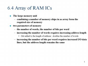
6.4 Array of RAM ICs
- The large memory unit
- combining a number of memory chips in as array
form the required size of memory - two parameters of memory
- the number of words, the number of bits per word
- increasing the number of words requires
increasing address length - 1bit added to the length of address doubles the
number of words - increasing the number of bits per word requires
increased I/O data lines, but the address length
remains the same
2
64K x 8 RAM chip
216 64K
In order to increase the number of memory words,
we use two or more RAM chips when 1 bit added
to the address, we can obtain double address
spaces 4 RAM chips adding 2 bits to the address
3
Constructing 256K x 8 RAM with 4 64K x 8 RAM chips
2 MSBs are used for selecting RAM chips
Total 218 256K
4
The same number of words, but with twice as many
bits in each word
- 64K x 16 RAM
Bidirectional I/O common terminals for the data
input and output
5
Arrays of dynamic RAM ICs
- DRAM controller performs addressing for DRAM
arrays - 1. Controlling separation of the address into a
row address and a column address - 2. Providing RAS and CAS signals
- 3. Performing refresh operation at the necessary
interval times - 4. Providing status signals for indicating
whether the memory is busy
6
6.5. Programmable logic technologies
- 4 types PLDs ROM, PLA, PAL, CPLD, FPGA
- 1. control connection
- fuse technology high current breaks the
connection(OPEN) - mask programming technology
- antifuse technology separated by high resistance
material - high voltage melt the material, then changed to
low resistance - these technologies make permanent connection
- if the programming is incorrect, the device must
be discarded - static RAM(SRAM) bit driving gate type
- if bit stores 1, then the transistor is turned ON
- this technology is volatile
- 2. building look-up tables
- logic is implemented simply by storing truth
table look-up table - 3. control of transistor switching
- storing charge on a floating gate of MOS
transistor - programming applies high voltage,
- erasure uses ultraviolet light source
7
6.6 ROM
- Permanent binary information is stored
32x8 ROM
8
Example of ROM
A7(I4 I3 I2 I1 I0 ) ?m(0, 2,3, ,29)
PROM programmable ROM EPROM erasable
programmable ROM EEPROM electrically erasable
programmable ROM
9
Combinational circuit implementation
- Decoder with k inputs generate the 2k minterms
- constructing Boolean function(Sum of minterm)
inserting OR gates - ROM is essentially a device that includes both
the decoder and the OR gates - ROM can be interpreted in two ways
- as a memory device
- as a circuit that implements a combinational
function previous example
Advantage of ROM usage not necessary the logic
diagram except for truth table
A7(I4 I3 I2 I1 I0 ) ?m(0, 2,3, ,29)
10
Example 6-1 Implementing a combination circuit
using a ROM
- Design a circuit accepts a 3-bit number and
generates an output binary number equal to the
square of the input number
11
Three major types of PLDs
12
6.7 PLA
- Difference from PROM
- Programmable AND Array
- example 3 inputs, 4 product terms, two outputs
F1 AB AC ABC F2 (AC BC)
13
Example 6-2. Implementing a combination circuit
using a PLA
- Sum of minterms
- F1(A, B, C) ?m(0, 1, 2, 4)
- F2(A, B, C) ?m(0, 5, 6, 7)
- Simplification
- F1 (AB AC BC)
- F2 AB AC ABC
14
6.8 PAL
feedback
PLD with fixed OR array and programmable AND
array easier programming, but not as flexible as
the PLA
15
Example 6-3 Implementing a combinational circuit
using a PAL
- W(A, B, C, D) ?m(2, 12, 13)
- X(A, B, C, D) ?m(7, 8, 9, 10, 11, 12, 13, 14,
15) - Y(A, B, C, D) ?m(0, 2, 3, 4, 5, 6, 7, 8, 10,
11, 15) - Z(A, B, C, D) ?m(1, 2, 8, 12, 13)
feedback
16
Connection map
Recommended
CrystalGraphics Presentations


