
3'3'4 BiCMOS Process Extensions - PowerPoint PPT Presentation
1 / 5
Title:
3'3'4 BiCMOS Process Extensions
Description:
CVD Tungsten-plug. retrograde wells. high angle lateral implants. shallow trench isolation ... CVD Tungsten-plug fills Contacts and Vias, and allows Contacts and Vias ... – PowerPoint PPT presentation
Number of Views:70
Avg rating:3.0/5.0
Title: 3'3'4 BiCMOS Process Extensions
1
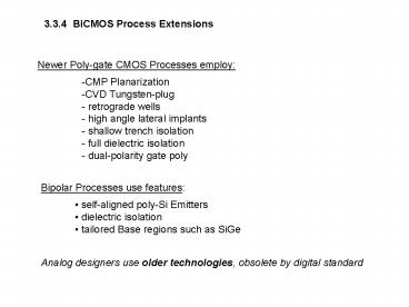
3.3.4 BiCMOS Process Extensions
Newer Poly-gate CMOS Processes employ
- CMP Planarization
- CVD Tungsten-plug
- retrograde wells
- high angle lateral implants
- shallow trench isolation
- full dielectric isolation
- dual-polarity gate poly
Bipolar Processes use features
- self-aligned poly-Si Emitters
- dielectric isolation
- tailored Base regions such as SiGe
Analog designers use older technologies, obsolete
by digital standard
2
Advanced Metal Systems
- BiCMOS here uses two-level metal, contact
silicidation, and etched vias - typical BiCMOS has etiehr 3 or 4 layers of metal
(100 nm refractory metal 500 nm Cu-doped Al) - CVD Tungsten-plug fills Contacts and Vias, and
allows Contacts and Vias to be stacked on top of
each other (called nesting). - All Contacts must have single uniform size.
This and refractory-silicides disable Schottky
contacts. - Most analog processes support Vop 10 20 V.
Dielectric Isolation (DI)
- Dielectric isolation is good for high speed, and
also for high voltage. - Deep wells required for 100-V or more D.I.
greatly reduces spacings between components - DI ensures
- no parasitic channels
- no minority carrier injection
- no substrate debiasing
- Accomplished by Wafer Bonding Trench Isolation
3
Different Trench Isolation of NPN Trench etch
occurs before Nwell diff.
- Most conservative NWell extends beyond Trench
- All junctions away from isolation
- NBL stops short of trench
- breakdown cannot occur along trench sidewalls
- requires more space than JI
- Somewhat more aggressive Junctions terminate
within trench - NWell terminates in Trench
- Greatly improves device packing, only minimal
risk - Good compromise between space saving potential
risks
- Still more aggressive Junctions intersect with
Trench sidewall - Base and Nwell drawn to middle of Trench
- CBJ intersects Trench sidewall
- Saves space, but CBJ crossing sidewall can show
low breakdown and high leakage
- Most aggressive multiple Junctions intersect
Trench sidewall - both CBJ and EBJ intersect Trench sidewall
- breakdown concerns
- high leakage due to surface recomb along sidewall
4
DI BiCMOS Process
- 1 um thick Oxide, followed by Wafer bonding of P-
Si - Polishing, oxidation, then NBL masks
- 10-um P-epi growth
- Thick CVD nitride, then Isolation mask
- Plasma etch for Trench
- Oxidation of Trench sidewalls
- Trench is filled with poly-Si
- Nitride stripped, surface polished
DI BiCMOS versus JI BiCMOS first few steps
5
DI BiCMOS vertical NPN
DI BiCMOS Vertical PNP
Recommended
CrystalGraphics Presentations


