
Analog to Digital Converters ADCs cont' - PowerPoint PPT Presentation
1 / 11
Title:
Analog to Digital Converters ADCs cont'
Description:
The time taken (T) by the refernce voltage will depend on the relative sizes of Vain and Vref ... Integrator starts integrating Vain. Counter starts counting. ... – PowerPoint PPT presentation
Number of Views:48
Avg rating:3.0/5.0
Title: Analog to Digital Converters ADCs cont'
1
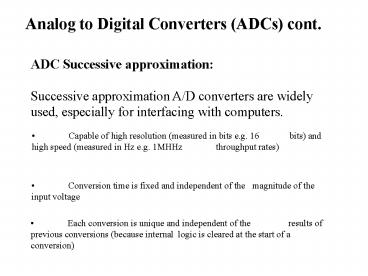
Analog to Digital Converters (ADCs) cont.
ADC Successive approximation Successive
approximation A/D converters are widely used,
especially for interfacing with computers.
Capable of high resolution (measured in bits
e.g. 16 bits) and high speed (measured in Hz
e.g. 1MHHz throughput rates)
Conversion time is fixed and independent of
the magnitude of the input voltage
Each conversion is unique and independent of
the results of previous conversions (because
internal logic is cleared at the start of a
conversion)
2
Block Diagram of Successive Approximation A/D
Converter
3
Conversion Techniques
Half Stepping Consists of comparing the unknown
input against a precise voltage (or current)
generated by a DAC.
Conversion command is applied The converter has
been cleared of previous conversion The DACs MSB
output is compared with the input (Note The MSB
output represents half the full scale 11112
1510, 10002 810(half way between 010 and 1510)
4
If input is Greater Than the MSB
A 1 is placed in the output register The next
bit is tried (Note The next bit output
represents quarter the full scale11112 1510,
01002 410 (quarter way between 010 and 1510)
If input is Less Than the MSB
A 0 is placed in the output register The next
bit is tried If that 2nd bit doesnt add enough
weight (voltage/current) to exceed the input, it
is left on (i.e. 1 in the output register,
and the next (third) bit is tried.
5
The process continues in order of descending bit
weight until the last bit is tried.
When the process is completed, the status line
changes to indicate that the contents of the
output register now constitute a valid conversion.
The contents of the output register form a binary
digital code corresponding to the input signals
magnitude.
6
During conversion, the input signal does not
change. If the input were to change during
conversion the output number could no longer
accurately represent the analog input.
Sample-hold device used to avoid this
problem. It is used ahead or the converter to
retain the input value that was presented at a
given time before the conversion starts, and
maintain it constant throughout the conversion.
Sample-hold device may not be needed if the
signal varies slowly enough and is sufficiently
noise-free that significant changes will not be
expected to occur during the conversion interval
7
Integrating Amplifier
What is the integral of a complete cycle of a
sinusoidal wave. ?sin ø
8
- If a sin wave is integrated over a period of time
equal to its periodic time will always integrate
to 0.
Mains noise
V
True sensor signal voltage
t
If we integrate the sensor signal noise for a
50th of a second then whatever we get as the
output voltage from the integrator will have no
mains noise ( as it would have integrated to 0)
9
- So what is the output of the integrator?
T time taken by the refernce voltage
t 1/50th sec
t
V
- At the end of the time t when our unknown analog
input voltage Vain has caused the output of the
integrator to swing down to some unknown value of
Vout, - we now switch the input of the integrator to a
negative reference voltage(Vref). - The output voltage should now start to ramp back
towards 0 Volts - The time taken (T) by the refernce voltage will
depend on the relative sizes of Vain and Vref - If t T then Vain Vref, t T/2 then Vain
Vref/2
10
DUAL SLOPE INTEGRATING ADC
Vref
Vain
11
Conversion Steps
- Convert Command comes from the computer
- Digital clock block, synthesizes input switch to
Vain, Sets the counter to 0, Sends out the Busy
signal at the status line - Integrator starts integrating Vain. Counter
starts counting. - Counter reaches max value (predetermined). And
then sets itself to 0 - Digital control now switches input to Vref.
Counter counts again. The output of the
integrator is now heading back to zero. - Integrator output reaches 0, Comparator output
flips causes the digital control to inhibit clock
pulses. Sends the output signal ready. Then the
computer reads the contents of the 8bit counter
Recommended
CrystalGraphics Presentations


