
Connectors, Vias and Stubs (some semi-random observations) - PowerPoint PPT Presentation
1 / 16
Title:
Connectors, Vias and Stubs (some semi-random observations)
Description:
After material loss effects, connector design and especially via ... Anti-pad enlargement. 2002 Teraspeed Consulting Group LLC. Page 5. TERASPEED. CONSULTING ... – PowerPoint PPT presentation
Number of Views:37
Avg rating:3.0/5.0
Title: Connectors, Vias and Stubs (some semi-random observations)
1
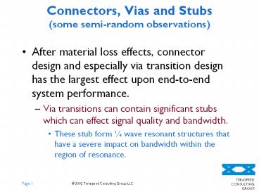
Connectors, Vias and Stubs(some semi-random
observations)
- After material loss effects, connector design and
especially via transition design has the largest
effect upon end-to-end system performance. - Via transitions can contain significant stubs
which can effect signal quality and bandwidth. - These stub form ¼ wave resonant structures that
have a severe impact on bandwidth within the
region of resonance.
2
Via Stubs
Connection from the connector PTH to the
backplane trace is made at the via
transition. Most transition types leave an open
via stub. This stub forms a high quality quarter
wave resonator whose resonant frequency is a
function of its length and material properties.
3
Via Stub SimulationsFR-4 vs. RO4350 for 30-inch
System
RO4350 with good via design
Poor via transition design can cause unwanted
stubs. These stubs for ¼ wave resonators, which
reduce and limit system bandwidth. Even though
Rogers 4350 material has superior loss properties
over FR-4, poor via transition design can negate
this performance advantage.
FR-4 with good via design
RO4350 with poor via design causes resonance
4
Via Stub Reduction
- Methods for reduction of via stub resonators
- Preferential routing to reduce stub length.
- Uses lowest routing layers. (Lowest cost with
performance relative to stub length.) - Counter-boring.
- Removes unwanted stubs by controlled depth
drilling as a final manufacturing step.
(Additional cost and manufacturing loss with
similar performance to buried vias. Difficult to
test!) - Buried Via Technology
- Additive laminate and laser drilling. (Highest
cost with highest potential performance.) - Reduction of Parasitic Capacitance
- Pad removal
- Anti-pad enlargement
5
Insertion Loss vs. Via Stub LengthFR-4
Via stub 0 to 150 mils. 8 mil 30-inch trace.
Longer stub
Note Internal stubs within connectors will also
limit performance in this way.
6
Insertion Loss vs Via ImpedanceRogers 4350
Via Impedance 35 to 50 ohms. 8 mil 30-inch trace.
Higher capacitance
Increased via capacitance leads to increased
impedance. These effectively load the via stub
structure and decrease the resonant frequency.
The reduction in resonant frequency is seen in a
loss in system bandwidth.
7
BGA Breakout Via Coupling Simulations
- CST Microwave was used to perform detailed
modeling and simulation of via breakout region
under BGA devices. - 3D Finite Integration Technique time-domain field
solver and simulator with bandwidth well beyond
50 GHz. - Field solver transforms time domain simulations
into frequency domain using Discrete Fourier
Transform of system stimulated with a Gaussian
pulse.
8
Via GeometrySide View
9
Via GeometryPerspective View
10
Via GeometryTop View
11
Time Domain Gaussian Pulse Simulation
12
S41 (Insertion Loss)
13
S42 (Crosstalk)
14
S43 (Crosstalk)
15
S11 (Return Loss)
16
FEXT Connector with Vias
With two coupled vias.
11 SignalGround With and without breakout vias.
Connector only.
Via-to-via crosstalk can easily exceed connector
crosstalk, when signal vias are not well
referenced and isolated by ground vias.