
AIR FORCE OFFICE OF SCIENTIFIC RESEARCH - PowerPoint PPT Presentation
1 / 13
Title:
AIR FORCE OFFICE OF SCIENTIFIC RESEARCH
Description:
Low capacitance better S/N for LADAR and Free-space Laser Comm. ... J. Chen, J. B. Khurgin and R. Merlin. Coherent LTA Phonon Generator. LTA Phonon Sink ... – PowerPoint PPT presentation
Number of Views:174
Avg rating:3.0/5.0
Title: AIR FORCE OFFICE OF SCIENTIFIC RESEARCH
1
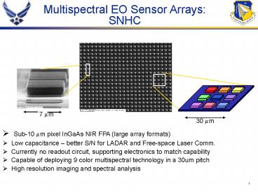
Multispectral EO Sensor ArraysSNHC
- Sub-10 mm pixel InGaAs NIR FPA (large array
formats) - Low capacitance better S/N for LADAR and
Free-space Laser Comm. - Currently no readout circuit, supporting
electronics to match capability - Capable of deploying 9 color multispectral
technology in a 30um pitch - High resolution imaging and spectral analysis
2
Resonant Tunneling MQW UV Detector
Structure of GaN/AlGaN MQW photodetector sample.
- Tunable High Efficiency Resonant Tunneling
GaN/AlGaN MQW UV Photodetectors - P.I. Institute Prof. R. R. Alfano at City
College of New York - Objective Develop UV photodetectors based on
III-Nitride MQW structures for high quantum
efficiency, tunable, fast and narrow bandwidth
response, and high signal-to-noise ratio. - Progress The first MQW UV detector sample was
designed, simulated, fabricated, and is under
test. - Industry Interaction SVT Associates Inc. is
interested in this research work.
Calculated photoresponse spectra by considering
different structure parameters.
3
Microstructured GaAs for QPM Stanford (SU)
Microstructured NLO Crystals for Infrared
Countermeasures (IRCM)
- Accomplishments
- Measured OP-GaAs NLO coefficient
- 5 x larger than mid-IR standard, PPLN
- Characterized dispersion of GaAs
- literature data inadequate
- results enable mid-IR source design
- Measured H2O line at 8 mm using
- OP-GaAs-based DFG system.
- Objectives
- - Develop engineerable bulk and thin film
microstructured III-V material for mid-IR
coherent sources - Apply to
- high-power mid-IR sources for IRCM
- spectroscopic sensors
- optical signal processing
- Collaborations
- Sandia National Lab, Livermore, CA,
- Spectroscopic sensors
- Air Force Research Lab, Sensors Directorate
- Hanscom AFB Bulk HVPE growth
- WPAFB Mid-IR OPOs
- Blue Leaf Communications, Sunnyvale, CA
- Nonlinear characterization
- OP-GaAs based OPOs for IRCM
- Air Force CARMA program
- BAE Systems (formerly Lockheed Martin)
- Northrop Grumman
- Participants at Stanford University
- Faculty M. M. Fejer, J. S. Harris, R. L. Byer
- Post-Doctoral Research Associate O. Levi
- Visiting Scholars T. Skauli and K. Vodopyanov
- Graduate Students T. Pinguet, X. Yu, P. Kuo
- Research Focus and Approach
- - Growth of orientation-patterned material
- - Characterization of material properties
- Device demonstrations
- Transfer technology to industrial collaborators
4
World Record 2.5 um Laser Diodes Performance
CW operation
- Applications
- Remote chemical sensing
- Infrared Countermeasures
- Laser Radar
- Active Imaging
- Battlefield Illumination
SUNY Stony Brook - Belenky
5
Laser Protection Materials MLPJ
Develop and characterize materials to protect Air
Force sensors from IR laser threats
Current Emphasis Damage and Jamming protection
against agile IR threats Wavelengths MW IR (3 -
5 mm) LW IR (8 - 12 mm) Pulse duration
nanoseconds and longer
Compound semiconductor
Detailed temperature dependent measurement of
charge carrier decay rates provides important
guide to material development
6
GaN/AlGaN FET High power microwave electronics
SiO2
S
G
D
AlGaN
D
D
GaN
AlN
Substrate (sapphire or SiC)
- operating frequencies 1-100 GHz (projected)
- large variations in electron concentration
within 2D channel - ? expect creation of large amplitude coherent
phonons - a potentially important channel of energy
dissipation
Initial studies by all-optical techniques
MURI2000
7
Quantum Dot Diffraction Grating for Coherent
Phonon Generation
Goal Generation of coherent phonons for phonon
annihilation
- AFM image of nano-pore template for
electrochemical assembly of quantum dot arrays.
Note high degree of regimentation. Balandin et.
al., Appl. Phys. Lett., 76, 137 (2000). - Strain-free structure Test-bed for numerical
modeling - Phonon carrier scattering can be tuned -
periodicity, acoustic mismatch, dot shape, etc. - Phonon-assisted optical transitions can be tuned
- Consider placement under gate enables GaN FET
8
Phonon Cooling Enhanced LO Decay by Stimulated
Emission
InP LO ? TO LTA 0.15 Strain ? 200 ps ? 10 ps
- J. Chen, J. B. Khurgin and R. Merlin
9
Collective Excitations Plasmons, Polaritons
- Effects/Applications
- II-VIs QW heterostructures can enhance
exciton-photon coupling. Combination of lower
dimensional gain medium, with micro-resonator
design, and excitation scheme can lead to
efficient low current density light emitter - Potential fluctuations in semiconductors may be
smoothed by extended exciton-polariton states - Optical waves propagating through nano-tunnels
are comprised of various coupled modes of surface
plasmon polaritons Takahara - Local polariton modes (LPMs) from strong
phonon-light interaction, results in splitting of
the LO and TO modes sensitive to changes in
local elastic constants around defects Foygel - Interference between two exciton-polariton
branches creates a grating of dielectric
polarization Malpeuch - Resonant Rayleigh scattering (RRS) detected
Rabi-oscillations in microcavities Malpeuch
10
Impact on Electronics
- Increased integration density, low noise, and
anticipated increase of power output for the same
device dimensions up to 25-50. - Field effect transistors
- Control the interaction between hot electrons in
FET channel and optical phonons - fully
characterize generated and injected phonons - Improve heat exchange - develop model describing
phonon dispersion modified by structure,
plasmons, injected coherent phonons... - Heterojunction bipolar transistors - Use
interaction with optical phonons, coupled
phonon-plasmon modes to decrease base resistance
to minority carriers - model effects on
performance - Resonant tunneling diodes - Use plasmon effects
from increased injection, required for higher
power, to enhance the device performance -
characterize plasmon under various conditions
11
Impact on Optoelectronics
- Quantum well lasers - investigate tradeoffs
between doping strategies and engineered plasmon
modes in cladding for improved confinement -
characterize cavity including plasmon layers,
high power (1W ) QW lasers, room temperature,
wide spectral range of 4 15 ?m - Quantum cascade laser
- Investigate plasmon line narrowing to counter
nonparabolicity and scattering - higher gain -
characterize effect - Investigate phonon-engineered depopulation of the
lower lasing level - model scheme for 10X
improvement - Determine conditions for high-speed operation
using intersubband transitions - modulation
frequency up to 300 GHz and power up to 100 mW at
room temperature - Quantum dot laser - control the homogeneous line
broadening due to the deformation potential from
acoustic phonons - model and predict the expected
improvement, output in 100s mW - Detectors - control the phonon mediated processes
governing carrier transport and capture in QW and
QD detectors, resonant plasmon screening field
and doping conditions for defect screening
12
Collective Excitations
- Develop physics of collective excitations and
transition into next generation of electronics
and optoelectronics - Physics complementary to engineering solutions -
example from thermal management - Phononics provide revolutionary approach to
increasing operating temperature of lasers and
detectors, rather than engineering by material
selection, doping profile, growth temp - Device structures are being investigated to
control phonon/electron scattering, use phonons
for laser pumping, develop coherent phonon
generation tool - Collective Excitations
- Concentrate on phonons, plasmons and their
interactions. Also polaritons interaction of
collective oscillations with electromagnetic
waves. - Addresses fundamental physics to extend
performance of broad classes of devices FETs,
HBTs, RTDs, semiconductor lasers and detectors
13
Semiconductor Materials Summary
- Broad range of materials are needed for a variety
of missions - Sensors - faster acquisition of diverse targets
over a wide range of conditions, efficient
devices - Lasers for active sensing and optical signal
processing - Organics for low-cost, flexible optoelectronics
- Chalcopyrites for access to higher power lasers
- Collective excitations - basis for next
improvements
Recommended
CrystalGraphics Presentations


