
MCNP Simulation - PowerPoint PPT Presentation
Title:
MCNP Simulation
Description:
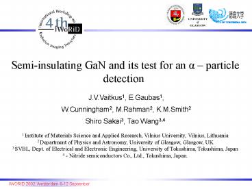
Semi-insulating GaN and its test for an particle detection J.V.Vaitkus1, E.Gaubas1, W.Cunningham2, M.Rahman2, K.M.Smith2 Shiro Sakai3, Tao Wang3,4 – PowerPoint PPT presentation
Number of Views:80
Avg rating:3.0/5.0
Title: MCNP Simulation
1
Semi-insulating GaN and its test for an a
particle detection J.V.Vaitkus1, E.Gaubas1,
W.Cunningham2, M.Rahman2, K.M.Smith2 Shiro
Sakai3, Tao Wang3,4 1 Institute of Materials
Science and Applied Research, Vilnius University,
Vilnius, Lithuania 2 Department of Physics and
Astronomy, University of Glasgow, Glasgow, UK 3
SVBL, Dept. of Electrical and Electronic
Engineering, University of Tokushima, Tokushima,
Japan4 - Nitride semiconductors Co., Ltd.,
Tokushima, Japan.
2
Outline
Introduction GaN I-V and I(t), Ds (t)
SI-GaN photoconductivity model a particle
detection spectra
3
GaN
Wurtzite polytype GaN Bandgap energy
3.44 eV (300 K) Density,
6.15 g/cm3 Breakdown field gt5 x 106
V/cm Electron mobility 1000
cm2/Vs Static Dielectric Constant
8.9 Lattice Constant
a3.189 c5.185 (Å) Zinc-blende structure
GaN Bandgap energy
3.2-3.3 eV (300 K) Lattice
constant a 4.52 (Å )
4
GaN samples The samples investigated were
epitaxial GaN layers grown by MOCVD on Al2O3
(0001) substrates. The layer properties were
changed by varying the substrate temperature and
trimethyl gallium (TMGa) flow rate. A
cross-section of the sample structure is given in
Fig. Ti/Al Ohmic contacts or Au Schottky type
contacts were used
The buffer n-GaN layer was 2 ?m thick. An
epitaxial capping layer 2.0-2.5 ?m thick was
grown at a different TMGa flow rate.
5
Combined measurements of I-V, time dependent
current characteristics and long-lived
photoconductivity relaxation were performed using
Keithley and HP electrometers. The sample was
biased between the contacts 1 and 2 or 1
and 3 (Fig.1). A white lamp source, light
emitting diodes of different wavelengths and
an 241Am radioactive source were used for
non-equilibrium carrier excitation.
6
I-V
Space charge limited current (SCLC)
Here e dielectric constant, e0 electric
constant, µn electron mobility, ? trapping
coefficient, L the sample thickness, U the
bias voltage. If a semi-insulatos is trap-free
mobility of electrons 10-40 cm2 / sV
Trap filling
Electron concentration at the contact 1014 - 1015
cm-3 or the high electric field effects.
7
I(t)
Red light on during sample bias off
Transient behaviour of dark current at different
bias voltages.
A current if the periodic sample bias on and off
8
The stretched exponent (dark current)
I(t) and I(0) are the current values at moment t
and at initial time, respectively, t
characteristic time constant for dark current, ß
decay exponent.
A better fit to I 0.4 exp(-t/350)0.496
, the initial part a sum of two exponents
time constans are 33.10.1 s and 1212 s and
partial amplitudes 0.0740.002, 0.5730.002,
respectively.
A fit to a single t 45 s,ß 0.33
According to a fractal diffusion model these ß
values show the existence of 1D or 2D random walk.
9
The stretched exponent (photocurrent)
I(t) and I(0) are the current values at moment t
and at initial time, respectively, t
characteristic time constant for dark current, ß
decay exponent.
10
GaN model
F. A. Ponce, in Introduction to nitride
semiconductor blue lasers and light emitting
diodes, Edited by S.Nakamura and S.F.Chichibu
(Taylor and Francis, 2000) p. 105.
11
GaN model
It is proposed that the observed phenomena can be
explained by including the compensation of
conductivity in the SI region and a change
of overlapping potential barriers that are
created by injected local charge and captured in
the defects related to the crystallite columns in
the layer.
12
Experimental arrangements for a fast photocurrent
response investigation
Measurement of microwave absorption transient
behaviour (the MW probe spot near field dimension
is about 100 and 500 ?m when using 22 and 10 GHz
instruments and implementing MW reflection or
absorption regimes, respectively) after
excitation by light pulse (NdYAG laser 2nd, 3rd
harmonics, blue LED). Probing provides a
photo-response that is proportional to
photoconductivity.
13
The fast components
Photoconductivity decay in different samples.
14
The fast components a dependence on T
The activation energy of the slowest component
gives a value for this barrier height that was
found equal to 0.14 eV. A similar value is
extracted from a comparison of the temperature
dependence of the asymptotic time constant 0.14
eV is the difference of activation energy between
samples 1-a and 2-a in Fig. The increase of
photoconductivity time constants shows that there
is multiple trapping of carriers as in the
Shockley-Read-Hall theory. Therefore it can be
proposed that the characteristic activation
energy of multiple trapping is 0.17 eV and 0.26
eV. The dependence of the initial component is
similar in both samples and it can be deduced
that the difference in absolute value is related
to the trap concentration in different samples.
Temperature dependence of (a) the fastest and
(b) the asymptotic components of
photoconductivity decay and (c) the relative
amplitude of the asymptotic component in samples
grown at 925 0C and TMGA flow rates g2 and g4,
(curves 1 and 2, resp.).
15
Alpha particle detection
Alpha particle detection
The radiation source Am241 were used for
non-equilibrium carrier excitation. The Am241
emits 5.48 MeV a particles.
The detector and source were housed in a vacuum
chamber.
16
The sample was biased between the contacts 1
and 3
17
Alpha particle detection
- Equipment
- a standard multi-channel analyser,
- comprising pre-amp, shaper,
- comparator and scalar, with a shaping time of 1
µs, a gain of 50 and a live time of 300 s
(corrected for the system dead time).
The ?-particle spectrum was well resolved even
if the detector was not biased, showing the
existence of material polarization. The weak
dependence of the signal on bias voltage show
evidence of full depletion in the detector but
also the existence of high field effects that
change the shape of the resolved ?-particle
spectrum. It shows the large difference of the
peak shape from the Gaussian profile that fits
the spectrum at low bias.
18
Alpha particle detection
The good resolution spectrum was measured up to
electric field 62 kV/cm. (I.e., up to bias 28
V, but the dark current was measured up to bias
100 V.)
19
- Summary
- This investigation of SI - GaN shows the
importance of space charge effects and traps on
the dark conductivity and photoconductivity. - Percolation effects were observed in the temporal
dependences of dark conductivity and
photoconductivity decay. - The well resolved ?-particle spectra gives the
promise of possible applications of this material
for the detection of ionizing radiation.
20
Authors express a gratitude to the Royal
Society and PPARC grants that supported a part of
this work and to Tokushima University Sattelite
Busines Venture Laboratory grant (J.V) .
21
Thank you for your attention !
Recommended
CrystalGraphics Presentations


