
Koc University - PowerPoint PPT Presentation
1 / 45
Title:
Koc University
Description:
Fourier Transform Spectrometer 2. MEMS Stages with Microlens arrays Portable Mid/Far IR Spectroscopy FTS : Lamellar Grating Interferometer Based MEMS Grating: ... – PowerPoint PPT presentation
Number of Views:232
Avg rating:3.0/5.0
Title: Koc University
1
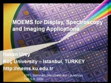
MOEMS for Display, Spectroscopy and Imaging
Applications
Hakan Urey Koç University Istanbul,
TURKEY http//mems.ku.edu.tr
EPFL Seminars (Neuchatel and Lausanne) Feb 5-6,
2009
2
- Koç University
- Private University established by Vehbi Koç
Foundation - 3,500 undergraduate and 400 MS and PhD students.
- Established in 1993 College of Engineering in
2001 - Among the top Universities in Turkey based on
scholarly research articles and faculty awards
3
Prof. Hakan Ürey (Director) Dr. V.C. Kishore
(Post-doc) Sven Holmström (Researcher) Selim
Ölçer (Technician) Graduate Students Onur
Ferhanoglu Aslihan Arslan Huseyin R. Seren Erdem
Erden Gökhan Hatipoglu S. Kutal Gökçe Duygu
Kutluoglu (KU-EPFL) Ersin Huseyinoglu Undergraduat
e Assistants Utku Baran Erman Timurdogan Özge
Tekin Baran Gözcü Özerk Memis F. Firat Gonen
- Research Focus
- Micro-optics,
- MEMS/NEMS sensors and actuators,
- 2D/3D Display and Imaging Systems
4
Outline OML Research Projects
- Brief Overview of
- MOEMS thermal sensor array
- 3D Displays ? Not MEMS
- Part 1 Electro-Magnetic Actuated Systems
- Pico projectors and 2D MEMS scanner (Lorentz
Force) - FR4 scanners for imaging (Moving magnet)
- MOEMS biosensors (Thin Ferromagnetic Film)
- Part 2 Comb-drive Electrostatic Actuated
Systems - MOEMS Fourier transform spectrometers
- Scanned Imaging using MEMS Stages and Microlens
Arrays
5
OML Research Projects MOEMS Thermal Imaging
Sensor Array
IR
- Advantages
- - Eliminates the need for electrical connection
- Interferometric sensitivity
- ?Recent collaboration with EPFL (Prof. Leblebici)
Licensed to ASELSAN, TR
JAP 2006 PTL 2008 SensAct 2009
6
Two-wavelength Interferometry for Extended Range
Imaging with Grating Interferometry
Unambigious detection Full range
O. Ferhanoglu, F. Toy, H. Urey, PTL 2007
7
OML Research Projects3D Display Development
Projects
Novel 3D display technology Scanning LED Array on
FR4 platform
Multi-viewer 3D display technology
G
Light engine module of the 3D display system
R
B
Sponsor EC FP7-STREP HELIUM3D
Sponsors TUBITAK FP6 3DTV
8
EM Actuated Devices
- MEMS Scanners ? Display
- FR4 Scanners ? Imaging
- Ni Cantilever Resonators ? Biosensor
9
Needs a MEMS Scanner
- Case for a scanning mirror laser light
- Together they address all the critical properties
- Small size
- Low power
- Bright
Light source
Single Mirror scanner
Image plane
10
Microvision PicoP MEMS Inside
CES2007
Integrated Photonics Module (IPM) Including 2D
MEMS scanner and modulated RGB Laser diodes
CES2008
2D MEMS Scanner
11
2D MEMS Scanner with Single Coil Magnetic
Actuation
Horizontal Scan Flexures (20 KHz)
Portion of 2D Raster Pattern for SVGA Display
Vertical Scan Flexures (60 Hz)
Drive coil
- Coil current carries excitation signals for both
axis (60Hz sawtooth 20KHz sine)
12
Microfabrication
Si Die
- 300um Silicon wafer
- Structure formed with DRIE
- Front Side
- Electroplated multi-turn coils
- PZR sensors on both flexures
- Al mirror
- Backside KOH etched to reduce weight
Packaged Device (no vacuum) Includes magnet under
Si die
Integrated PZR Angle Sensor
R. Sprague et al Proc. SPIE Vol. 5721, pp. 1-13
(2005) Urey et al, Optical MEMS 2006
Yalcinkaya et al, JMEMS (2006)
13
Summary MEMS Scanner Performance Comparison
Horizontal Resolution
Yalcinkaya, Urey, Montague, Brown, Sprague,
JMEMS (2006)
Vertical Resolution
14
- Silicon MEMS scanners work great but making
really low-cost and low-frequency devices proved
to be difficult with Silicon!
In the middle of difficulty lies great
opportunity Albert Einstein
15
FR4 Scanners
16
FR4 as an Opto-Electro-Mechanical Platform
FR4
FR4 sandwiched between copper laminates
- Standard PCB technology
- Excellent electrical, mechanical, and thermal
properties - Different structural thicknesses 130um, 200um,
250um, 300um1.5mm - Highly integrated, flexible, robust, low-cost
17
High Degree of Integration on mm/cm-sized FR4
Platform (not possible with MEMS)
Fresnel lens and curved mirror on FR4 for imaging
LED array and focusing leng on FR4 (Module for a
3D display)
Integrated module with optics, IC,
optoelectronics, 2 DOF scanning
LED and waveguide on FR4 (displays / optical
interconnects)
18
Moving Coil with Lorentz Force Actuation
5mm x 5mm
Typically lt 200Hz operation
Electrical vias
Double-sided Cu coils
FR4 substrate
Mirror attached on one side
Urey et al, PTL 2008
19
FR4 Applications Imaging with Dynamic Focusing
? Moving LD mounted on FR4
500 um
75 mm
LD
f 6 mm
650 mm
LD
- 500 um displacement of the laser diode results
in about 600mm displacement of the focused spot
position - Can think of as either auto-focus OR x-z scanning
device
20
FR4 Laser Scanner with Dynamic Focusing
Experimental Results -
- As the spot is focused further away, spot size
gets bigger, DOF gets longer - 500um plunger displacement shifts the beam waist
location from 70mm to almost 700mm
Isikman, et al, PTL 2009
21
FR4 and Silicon Technology Comparison for EM
Actuators
FR4
Silicon
Fabrication Technology
Standard PCB
MEMS
Density kg/m3
1860
2300
Density of copper
8960
8960
Young's Modulus Gpa
10-20
168
Torsional Modulus Gpa
2-5
51
100um (drill) 20um laser (5um in 2009)
2um (lithography)
Min feature size
100um
Min Coil Trace Width / Spacing
10um
350um (25um with laser)
difficult
Min Via Hole Size
Copper thickness
30um
10um
Number of Coil layers
2 - 20
1
Resistance / Power
Low
High
22
Type 3 Thin Film Magnetic Actuatorsand MOEMS
Biosensor
23
Understanding Soft Magnetic Thin-Film Actuators
Push region
Pull region
Torque ? M H- Where M ? max (Hr, Msat)
- FACT Unlike thick magnetic films, force can be
attractive or repulsive. - WHY? Magnetization vector remains in-plane due to
strong shape anisotropy and the whole structure
rotates instead of magnetization - FACT Unlike permanent magnets, force is NOT
bidirectional - WHY? Changing current direction, rotates both H
and M vectors 180degrees, thus force direction
remains the same
24
Modeling Soft Magnetic Thin Film as Array of
Permanent Magnets
Thin magnetic film in external magnetic field
Integrated planar coil
Attractive to use magnetic thin films such as Ni
or NiFe as structural MEMS/NEMS layer.
Isikman et al, JSTQE 2007 Isikman, et al, IEEE J.
Magnetism (accepted) ? about dynamics
hysteresis modeling
25
New Actuator Model for High-Permeability Thin
Film Actuators
The magnetic layer is modeled as an array of
permanent magnets
Isikman et al, IEEE JSTQE 2007
26
New Model Validation for Permalloy Thin Films
- Model can handle
- Non-uniform fields
- Saturated/unsaturated film
y9
y-4
Isikman, Ergeneman, Yalcinkaya, Urey, IEEE JSTQE
2007
27
MEMS Chemical/Bio Sensors
- Interactions
- Steric
- Electrostatic
- van der Waals
Thundat et al. (ORNL), APL94 Chen et al., J.
Appl. Phys (1995).
28
Biosensor Research at Koc University
TÜBITAK
Dynamic Mode Actuation Use magnetic material as
structural material instead of Si or
SiN Detection Optical using integrated grating
interferometer
Blood sample
Functionalized cantilever array (parallel
operation)
Disposable MEMS Chip
Reflector for optical readout
EM actuation coil / Optoelectronics module for
readout
Electronics control/readout
Protein-ligand interaction changes the dynamics
of Micro/nano cantilevers
29
Diffraction Grating Readout
PD0
PD1
0th
-1st
1st
3rd
-3rd
Grating
NiFe cantilever
gap
Si substrate
Electro-coil
Gap / l
- Grating pattern can be on the moving or fixed
structure - Extremely sensitive can detect mechanical
deflections on the order of 2x10⁻⁴A/Hz½ at 20KHz.
Used for AFM and acoustic sensing IR sensing
Ferhanoglu, Toy, and Urey, PTL 2007 Degertekin,
et.al. JSTQE 2004 (Georgia Tech)
30
Simple Microfabrication
100um
Silicon Au Ni PR
5-10um
Si (doped)
Ni or NiFe
Photoresist
Remove PR
Mask
Isotropic Silicon Etching
- Magnetic actuation of Nickel thin film (1um
thick)
In collaboration with Profs. E. Alaca and H.
Kavakli at Koc University
31
Fabricated Cantilevers with Diffraction
Gratings(Fabricated in our clean room)
? They all work despite not so great surface
quality ? Thanks to AC-coupled detection, and
bias/noise rejection of diffraction grating
readout,
Ozturk et al, PTL 2008
32
Bio-detection Results
Resonance frequency shift of a cantilever due the
attachment of human kappa opioid receptors (hKOR)
to the Au surface. 180Hz shift ? 85pg of mass
SENSITIVITY is GOOD, future work will focus on
improving SPECIFICITY
Ozturk et al, PTL 2008
33
Comb Actuated Devices 1. Fourier Transform
Spectrometer2. MEMS Stages with Microlens arrays
34
Portable Mid/Far IR Spectroscopy
- FTIR spectroscopy is the common choice due to
single detector operation - Requirements for compact FTIR Spectrometers
- Translating mirrors with long travel range
- Precision scanning
- Real-time operation
- Large clear aperture
- Approaches
- Michelson interferometer
- Lamellar grating interferometer (eliminates beam
splitter and reference mirror, more compact)
Koc Univ., TR
U. Neuchatel, CH
Faunhofer IPMS, DE
35
FTS Lamellar Grating Interferometer Based
Grating Side View
l/a
a
0
-l/a
Monochromatic Light
36
MEMS Grating Features
- Comb fingers function as grating, actuators and
position feedback - Large clear aperture and good optical efficiency
- Simple fabrication process
Dimensions of the Device
Technology Licensed to Fraunhofer IPMS
37
Spectral Measurements
Measured Narrowband Spectrum
FTS Measurement l638.8nm, DlFWHM 24
nm Commercial visible spectrometer l638.8nm
DlFWHM 1.5 nm
FTS Theory Dl 2.3nm for 30um deflection
Photodetector Signal
Measured Broadband Spectrum
Ataman, Urey, Wolter, J. Micromechanics and
Microengineering, Vol. 16, p. 2517, 2006
38
Currrent and Future Work in this area
- MEMFIS Project Ultrasmall MEMS FT-IR
Spectrometer started in 2008 (funded by EC-FP7) - Develop a MEMS based compact FTS with lt10cm-1
spectral resolution for mid and long IR
applications
www.memfis-project.eu
39
Scanned Imaging using MEMS Stages and Microlens
Arrays(Microfabrication 2nd run planned at EPFL
clean rooms)
40
Scanning with MLAs
PSL
FL
DMLA
MLA1
laser
- Beam steering is possible by laterally moving a
collimating lens wrt focusing lens - Using microlens arrays (MLA) allows for large
angle steering with small lateral displacements - However, beam steering with MLA has a
fundamental diffraction related problem! - Can address only discrete angles set by period of
MLA - Our group showed that moving PSL and MLA1 in
SYNC allows for continuous addressing!
A. Akatay, C. Ataman, H.Urey, Optics Letters, 31
(19), 2861-2863, 2006.
41
Demonstrated Continuous Scanning with Microlens
Arrays
40 discrete addressable spots Using 650um clear
aperture
Can fit 150 spots with continuous
addressing gt1000 resolvable spots using Higher
f lenses and 2mm clear aperture
Akatay, Ataman, Urey, Optics Letters,
2006 Akatay, Urey, Optics Express, 2007
(l0.532mm) and the beam size is around 600mm
pitch (d) 200mm
42
MOS Fabricated Devices
- Fabricated at Chalmers University
- 20 mm and 50 mm thick (SOI)
- Fabrication process similar to 1st gen. MEMS
spectrometer
SEM Pictures
Microscope Pictures
43
Fabricated MLAs
- Replicated on 20 mm thick Cytop layer
- 100 Fill Factor
- 75mm pitch size
- f/4 (300mm f. length)
- Embossed using KS SB6 Wafer Bonder
- New fab run planned at EPFL (Feb-April 2009)
Hedsten et. al., MME 2008 (Koc and Chalmers
collaboration)
44
Summary Remarks
- MOEMS (i.e., moving micromechanical structures
combined with laser light sources and
micro-optics) is a powerful technology and
enables a number of applications - Thermal sensors, 2D and 3D Displays, Bio-sensors,
Spectroscopy, and Imaging are some of the
applications explored at Koc U. - 3-types of EM actuators are discussed moving
coil, moving-magnet, and soft-magnetic film.
Selection depends on application. - Best reported MEMS Scanner performance is
achieved using bi-magnetic Lorentz force
actuator. Suitable for pico-projector
applications. - FR4 mechanical properties and integration with
optics not explored before - offers low-cost and high degree of integration
- good choice for many applications 3D displays,
FTS, advanced imaging with dynamic focusing, etc. - Comb-actuated in-plane and out-of-plane moving
platforms are utilized for high-performance FTS
and beam steering applications - Comb actuation provide compact form-factor and
low-power. - Mechanical coupling provides an interesting way
to actuate, can be used both for EM and ES
actuated MEMS devices.
45
Acknowledgments
- All the past and current students and researchers
at OML - Funding Resources
- Microvision Inc. (USA)
- FP6 Projects NEMO, 3DTV, MC2ACCESS,
MINOS-Euronet - FP7 STREP Projects MEMFIS, HELIUM3D
- ASELSAN Inc. (Turkey)
- Fraunhofer-IPMS (Germany)
- TÜBITAK (Scientific and Technical Research
Council of Turkey) - TÜBA-Distinguished Young Scientist Award, Turkey
- NSF (USA)
- MEMS / Micro-Optics / 3D Displays
- Post-doctoral research positions available
- PhD positions available
Recommended
CrystalGraphics Presentations


