
Micro-Mechanical cleaving process to make nGLs - PowerPoint PPT Presentation
1 / 1
Title:
Micro-Mechanical cleaving process to make nGLs
Description:
Graphene shows high contrast in white light illumination for ~ 100 nm thick SiO2 Transport in FET geometry for nGLs shows Dirac peak with finite resistance. – PowerPoint PPT presentation
Number of Views:28
Avg rating:3.0/5.0
Title: Micro-Mechanical cleaving process to make nGLs
1
G
2DG
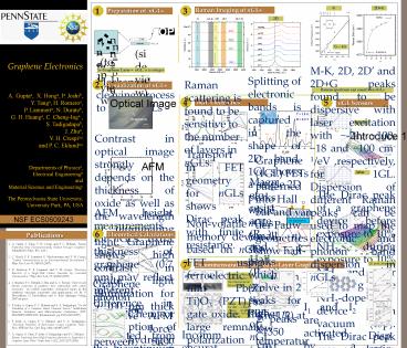
Raman Imaging of nGLs
Preparation of nGLs
2D
HOPG
n2
n5
n8
SiO2 Si
G 1/n
n1
n19
(side view)
(top view)
Micro-Mechanical cleaving process to make nGLs
M-K, 2D, 2D and 2DG peaks found to be
dispersive with laser excitation with -21, 100,
18 and 100 cm-1/eV ,respectively, for 1GL.
Dispersion of different Raman peaks can be used
to map the electronic and phonon band dispersion
in nGLs
n-Graphene Layer nGL n is integer
Splitting of electronic bands is captured in the
shape of 2D band. 1GL shows a single 2D peaks
while nGLs (small n) show 4 peaks which evolve
in 2 peaks for higher n.
Raman scattering is found to be sensitive to the
number of layers in nGLs.
Visualization of nGLs
Raman spectrum can count n in nGLs
Optical Image
nGL Electronics
nGL Sensors
Graphene
Before
Contrast in optical image strongly depends on the
thickness of oxide as well as the wavelength of
illuminating light. Graphene shows high contrast
in white light illumination for 100 nm thick
SiO2
Transport in FET geometry for nGLs shows Dirac
peak with finite resistance.
Graphene (1GL) FETs patterned into Hall bar and
van der Pauw geometries show half-integer quantum
Hall sequence 4(n1/2) at low temperature.
AFM
After
Magneto-resistance (Rxx) and Hall (Rxy)
measurements of nGL (ngt1) devices at low
temperature.
The Dirac peak of a graphene device before
exposure to 10 NH3, during exposure to 10 NH3
and after annealing the NH3-doped device in
vacuum (top). The Dirac peak recovery during
vacuum annealing of a different graphene device
exposed to Cl2(bottom)
S
D
nGL
AFM height measurements for nGLs. Extra thickness
of graphene (0.7 nm) may reflect inherent
difference in attractive AFM tip force between
SiO2 and graphene
200-400 nm PZT
Non-volatile memory device based on nGL-FET using
ferroelectric film Pb(Zr Ti)O3 (PZT) as gate
oxide. The large remnant polarization field of
PZT ( 40 µC/cm2) can potentially induce
enormous 2D carrier doping (3x10¹⁴/cm2) and lead
to non-volatile memory effect. Pronounced
hysteresis in carrier density and resistivity as
a function of Vg with long retention time is
observed in our nGL-FET.
Nb doped SrTiO3
Theoretical Calculations
Publications
- A. Gupta, Y. Tang, V. H. Crespi and P. C. Eklund,
Raman Scattering form Incommensurately Stacked
Bi-Layer Graphene Submitted to Phys. Rev. Lett.) - C. Nisoli, P. E. Lammert, E. Mockensturm and V.
H. Crespi, "Carbon Nanostructures as an
Electromechanical Bicontinuum," Phys. Rev. Lett.
99, 045501 (2007). - D. Stojkovic, P. E. Lammert and V. H. Crespi,
"Electronic Bisection of a Single-Wall Carbon
Nanotube by Controlled Chemisorption," Phys. Rev.
Lett. 99, 026802 (2007) - J. Charlier, P. C. Eklund, J. Zhu and A. C.
Ferrari,Electron and phonon properties of
graphene their relationship with carbon
nanotubes,'' in Carbon nanotubes Advanced topics
in the synthesis, structure, properties and
applications, ed. M. S. Dresselhaus, G.
Dresselhaus and A. Jorio (Springer Verlag, 2007)
in press - P. Joshi, A. Gupta, P. C. Eklund and S. A.
Tadigadapa,"On the Possibility of a Graphene
Based Chemical Sensor," Solid-State Sensors,
Actuators and Microsystems Conference, 2007.
TRANSDUCERS 2007. International , pp.2325-2328
(2007) - P. Joshi, A. Gupta, P. C. Eklund, and S. A.
Tadigadapa, Electrical Properties of Back-Gated
n-Layer Graphene Films, Proc. SPIE Int. Soc.
Opt. Eng. 6464, 646409 (2007) - A. Gupta, G. Chen, P. Joshi, S. Tadigadapa and P.
C. Eklund, Raman Scattering from High-Frequency
phonons in Supported n-Graphene Layer Films Nano
Lett. 6 (12), 2667-2673 (2006)
Incommensurately Stacked Bi-Layer Graphene
2D peak dispersion
Optical Image and Schematics of incommensurate
bilayer (IBL)
Graphene phonon dispersion curves calculated from
the bicontinuum theory (solid lines), compared to
EELS data. The bi-continuum theory of graphene
provides a unified treatment of a wide range of
electromechanical couplings well beyond that
accessible to a traditional single-continuum
(i.e. elastic) model.
I1 and I2 are activated by a superimposed
potential stemming from the I stacking. Peak at
1350 cm-1 found to be dispersive with excitation
energy while 1384 cm-1 is non dispersive. Peak
strength and dispersive behavior is understood
(right) by perturbing potential from one layer on
another by calculating the matrix element between
suitable electronic states
Band splitting for IBL 6 meV (Vienna Ab-initio
Simulation Package calculation)
Chemisorption of hydrogen can generate
well-defined graphenic bi- ribbons which access a
new regime of electronic coupling wherein
characteristic phonon energies exceed the
characteristic electronic energy scales for band
dispersion and inter-ribbon coupling.
2 peaks 1350 cm-1 and 1384 cm-1 (I1 and I2) are
seen in IBL and compared with defect induced D
band peaks (1 peak for mono graphene layer and 4
peaks for commensurate bi layer) at the edges of
nGLs.
Incommensurate stacking of two graphene layers
produces a pair of almost decoupled graphene
layers
Dispersion of 2D peak for 1GL, IBL and 2GL.
Recommended
CrystalGraphics Presentations


