
Transistor Basics - PowerPoint PPT Presentation
1 / 12
Title:
Transistor Basics
Description:
Collector. Ic, , mA. Forward active region. VCE. 70 A. Increasing Ib. NPN BJT. NPN BJT. B ... All devices are sized to fit the default grid. V1. I1. Q23. R23 ... – PowerPoint PPT presentation
Number of Views:684
Avg rating:3.0/5.0
Title: Transistor Basics
1
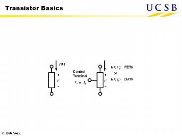
Transistor Basics
I(V)
I(V, Vc)
FETs
Control Terminal
or
I(V, Ic)
BJTs
V
V
Vc or Ic
2
JFETs
Drain
N-ch JFET
Drain
Gate
Vds
Ids(Vgs,Vds)
Gate
Vgs
Source
Source
Ohmic or Triode region
Saturation region
ID
N-ch JFET
Vgs 0
Idss
Id
Ig 0
D
Vgs Vt 1.5
Increasing Vgs
Vds
G
Vgs Vt 1.0
Vgs
S
Vgs Vt 0.5
Vds
Vgs Vt (cutoff)
3
MOSFET
Drain
NMOS
Drain
Gate
Vds
Ids(Vgs,Vds)
Gate
Vgs
Source
Source
Ohmic or Triode region
Saturation region
ID
NMOS
Vgs Vt 2.0
Id
Ig 0
D
Vgs Vt 1.5
G
Increasing Vgs
Vds
Vgs Vt 1.0
Vgs
S
Vgs Vt 0.5
Vds
Vgs Vt (cutoff)
4
Family Tree
5
BJTs
C
NPN BJT
Ib
IcaFIE
Ib
C
Collector
B
IcßIB
Base
B
IE
Emitter
E
E
Ic, , mA
Forward active region
70 µA
60 µA
NPN BJT
8
50 µA
Ic
6
40 µA
Increasing Ib
Ib
vcb
30 µA
4
vce
20 µA
2
10 µA
vbe
Ie
0 µA
VCE
Vce,sat
6
JFET Experiments
A
12 V
Ids
Drain
R D
Gate
Vds
Vout
Vgs
Id
Source
Vgs
RS ?
12 V
R ?
Id
Vg ?
Vout
7
MOSFET Experiments
2N7000
A
ID
Drain
Gate
Vds
3 V
Vgs
Source
1 µF
8
MOS CMOS
10 V
VDD
VDD
R D
PMOS
Vout
Vin
Vout
Vin
Vin
5 V
RS
R L
R L
NMOS
0 V
10 V
10 V
R D
1 k?
3 M?
Vout
Vout
Id
Vin
5 V
Vgs
0 V
R g
200 ?
9
CD4007
2
14
11
1
13
3
6
12
10
5
8
4
7
9
10
2N3904
2N3904
200µA
175µA
150µA
125µA
Collector Current, Ic Amps
100µA
Ib
75µA
50µA
25µA
0µA
Collector-Emitter Voltage, Vce Volts
11
2N3906
2N3906
200µA
175µA
150µA
125µA
Collector Current, Ic Amps
100µA
Ib
75µA
50µA
25µA
0µA
Emitter-Collector Voltage, Vec Volts
12
BJT Experiments
2N3904
10 V
Rc ?
Ic
5 V
Vout
Rb ?
2N3904
5 V
Rb
2N3906
5 V
Rc
Vin
5 V
Rc
0 V
Rb
f 1 Hz
2N3904
Recommended
CrystalGraphics Presentations


