
Lab 9: Matrix Keypad : PowerPoint PPT Presentation
1 / 3
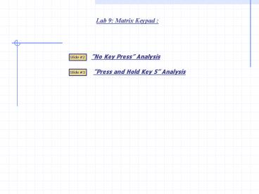
Title: Lab 9: Matrix Keypad :
1
Lab 9 Matrix Keypad
No Key Press Analysis
Slide 2
Press and Hold Key 5 Analysis
Slide 3
2
Lab 9 No key pressed Analysis
A matrix keypad has its keys arranged in rows
and columns. When a key is pressed it connects a
column to a row. Each key pressed is identified
by a unique column number row number connection.
Note The effects of switch bounce are ignored.
The AND gate will pass the 1 K PPS pulse waveform
to the clock input of the MOD 16 counter because
the control input is logic 1.
We will analyze the system with no key being
pressed down. All switches are open circuits. The
4 resistors pull up the inputs of the MUX to 5V.
Thus MUX Z1 regardless of the logic levels at S0
and S1.
The 1 of 4 decoder receives the quick changing
signals from the counter. The decoder is driven
by the mod 4 section. A1 A0 O0 O1 O2
O3 0 0 0 1 1 1 0
1 1 0 1 1 1 0 1
1 0 1 1 1 1 1
1 0 Continue and you will see a slow motion
animation of the decoder output cycling. Use the
backspace key to re-run the animation a few times
and you will see that net result is a logic 0
moving across the columns of the keypad from left
too right. The actual speed is much faster the
logic 0 moves right every millisecond.
The rotating logic 0 from the decoder does not
get transferred to the MUX inputs because all
keys are open circuit (not pressed). The MUX
inputs are selected one at a time and transferred
to Z. The MUX select inputs receive the quick
changing signals from the counter (Q2, Q3). A
different channel is selected every 4
milliseconds S1 S0 Z 0 0 I0
0 1 I1 1 0 I2 1 1
I3 Continue and you will see a slow motion
animation of the MUX cycling. Use the backspace
key to re-run the animation a few times and you
will see that net result is each keypad rows
logic level is transferred to Z every 4
milliseconds.
The data register receives the quick changing
signals from the counter. With Clk 1 the 4 bit
number at Da Dd is ignored by the data
register. The cycling from the counter is thus
ignored. Lets assume that the initial number
stored into the data register was 0. The end
result is The 0 gets displayed and the changing
signals from the counter are ignored.
Slide 2
3
Lab 9 Press and hold key 5
The demonstration will assume the counter starts
at 0 when the user presses and holds down key 5
of the matrix keypad. The actual time it takes
the system to respond to this event is 6
milliseconds. Lets also assume the data register
has 0 stored.
The 1 of 4 decoder receives 0,0 from the counter
and grounds O0 (active low). The other 3 outputs
remain at 1 (inactive). The logic 1 at O1 is
transferred through the pressed key to I1 of the
MUX.
The MUX inputs I0, I2, I3 are all at logic 1
because the keys on those rows are open and pull
up resistors make the input voltage 5V. The
result is MUX Z1.
- With MUX Z1.
- Data reg. Clk 1. Data reg. is disabled. It
ignores inputs DaDd and continues to display the
number 0 which is stored in the data register. - The 1 K PPS pulse is passed by the AND gate and
the counter rolls forward to 1.
The 1 of 4 decoder receives 0,1 from the counter
and grounds O1 (active low). The other 3 outputs
remain at 1 (inactive). The logic 0 at O1 is
transferred through the pressed key to I1 of the
MUX.
The MUX inputs I0, I2, I3 are all at logic 1
because the keys on those rows are open and pull
up resistors make the input voltage 5V. Even
though I10 the MUX output Z stays at logic 1
because the logic level at I0 is selected
(counter Q3, Q2 0,0)
- With MUX Z1.
- Data reg. Clk 1.Data reg. is disabled. It
ignores inputs DaDd and continues to display the
number 0 which is stored in the data register. - The 1 K PPS pulse is passed by the AND gate and
the counter rolls forward to 2.
The 1 of 4 decoder receives 1,0 from the counter
and grounds O2 (active low). The other 3 outputs
remain at 1 (inactive). The logic 1 at O1 is
transferred through the pressed key to I1 of the
MUX.
- With MUX Z1.
- Data reg. Clk 1. Data register is disabled. It
ignores inputs DaDd and continues to display the
number 0 which is stored in the data register. - The 1 K PPS pulse is passed by the AND gate and
the counter rolls forward to 3. - The counter continues to roll forward from 3 to 4
because the MUX Z1. Lets look ahead to when
the counter reaches 5 (the key number!).
The 1 of 4 decoder receives 0,1 from the counter
and grounds O1 (active low). The other 3 outputs
remain at 1 (inactive). The logic 0 at O1 is
transferred through the pressed key to I1 of the
MUX.
The MUX select inputs S1, S0 0,1. Channel I1
is selected and the logic 0 is passed to output
Z.
The AND gate will block the clock because Z0. It
stops the counter at the number 5.
Data reg. Clk changes to 0 because Z0. The data
register is clocked and the number 5 from the
counter is stored and displayed.
1
0
1
0
0
Slide 3
Recommended
