
Table of Contents - PowerPoint PPT Presentation
1 / 67
Title:
Table of Contents
Description:
3. Some Other Aspects of Pulse Shaping. 5. Digitization of Pulse and Time ... Use voltage pulse (can be measured conveniently with oscilloscope) ... – PowerPoint PPT presentation
Number of Views:66
Avg rating:3.0/5.0
Title: Table of Contents
1
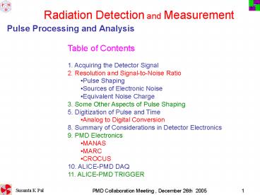
Radiation Detection and Measurement
Pulse Processing and Analysis
- Table of Contents
- 1. Acquiring the Detector Signal
- 2. Resolution and Signal-to-Noise Ratio
- Pulse Shaping
- Sources of Electronic Noise
- Equivalent Noise Charge
- 3. Some Other Aspects of Pulse Shaping
- 5. Digitization of Pulse and Time
- Analog to Digital Conversion
- 8. Summary of Considerations in Detector
Electronics - 9. PMD Electronics
- MANAS
- MARC
- CROCUS
- 10. ALICE-PMD DAQ
- 11. ALICE-PMD TRIGGER
2
Radiation Detection and Measurement
Pulse Processing and Analysis
A Typical Detector System
Processes in Scintillator - Photomultiplier
3
Signal Processing
1. Acquiring the Detector Signal
- Determine energy deposited in detector
- Detector signal generally a short current pulse
- Typical durations
- Thin silicon detector
- (10 ... 300 mm thick) 100 ps 30 ns
- Thick (cm) Si or Ge detector 1 10 ms
- Proportional chamber (gas) 10 ns 10
ms - Gas microstrip or microgap chamber 10
50 ns - Scintillator PMT/APD 100 ps 10 ms
4
- Necessary to integrate Detector Signal Current
Possibilities 1. Integrate charge on input
capacitance 2. Use integrating (charge
sensitive) preamplifier 3. Amplify
current pulse and use integrating (charge
sensing) ADC
DETECTOR
AMPLIFIER
velocities of charge carriers
rate of induced charge on detector electrodes
signal charge
Magnitude of voltage depends on detector
capacitance!
5
In reality the current pulses are more
complex. Current pulses on opposite sides
(n-strip and p-strip) of a double-sided silicon
strip detector (track traversing the detector)
n-Strip Signal, n-Bulk Strip Detector Vdep 60V,
Vb 90V
p-Strip Signal, n-Bulk Strip Detector Vdep 60V,
Vb 90V
Time ns
Time ns
Although both pulses originate from the same
particle track, the shapes are very different.
6
However, although the peak voltage or current
signal measured by the amplifier may be quite
different, the signal charge
is the same.
n-Strip Charge, n-Bulk Strip Detector Vdep 60V,
Vb 90V
p-Strip Charge, n-Bulk Strip Detector Vdep 60V,
Vb 90V
Time ns
Time ns
7
When the input time constant RC is much greater
than the signal duration, the peak voltage is a
measure of the charge
- The measured signal depends on the total
capacitance at the input. - In system where the detector capacitance varies,
e.g. - different detector geometries
- (e.g. strip detectors with different lengths)
- varying detector capacitance
- (e.g. partially depleted detectors)
- Use system whose response is independent of
detector capacitance.
2. Active Integrator (charge-sensitive
amplifier) Start with inverting voltage
amplifier
Voltage gain
Input impedance
(i.e. no signal current flows into amplifier
input)
8
Connect feedback capacitor
between output and input.
Gain
What fraction of the signal charge is measured?
Example
9
Calibration Inject specific quantity of charge -
measure system response Use voltage pulse (can be
measured conveniently with oscilloscope)
Voltage step applied to test input develops over
CT
Accurate expression
Typically
Realistic Charge-Sensitive Preamplifiers The
preceding discussion assumed idealized amplifiers
with infinite speed. In reality, amplifiers may
be too slow to follow the instantaneous detector
pulse. Does this incur a loss of charge?
10
Equivalent Circuit
Signal is preserved even if the amplifier
responds much more slowly than the detector
signal. However, the response of the amplifier
affects the measured pulse shape.
AMPLIFIER
DETECTOR
charges moving in detector induce change of
charge on detector electrodes
detector capacitance Discharges into amplifier
- How do real amplifiers affect the measured
pulse shape? - How does the detector affect amplifier response?
A Simple Amplifier
Voltage gain
high freq.
low freq.
upper cutoff frequency
11
Pulse Response of the Simple Amplifier A voltage
step vi (t) at the input causes a current step io
(t) at the output of the transistor. For the
output voltage to change, the output capacitance
Co must first charge up. The output voltage
changes with a time constant
The time constant t corresponds to the upper
cutoff frequency
12
Input Impedance of a
Charge-Sensitive Amplifier
Amplifier gain vs. frequency beyond the upper
cutoff frequency
Gain-Bandwidth Product
Input Impedance
Feedback Impedance
Imaginary component vanishes
Resistance
low frequencies
capacitive input
high frequencies
resistive input
13
Basic Noise Mechanisms Consider n
carriers of charge e moving with a velocity v
through a sample of length l. The induced current
i at the ends of the sample is
The fluctuation of this current is given by the
total differential
- where the two terms are added in quadrature since
they are statistically uncorrelated. - Two mechanisms contribute to the total noise
- velocity fluctuations, e.g. thermal noise
- number fluctuations, e.g. shot noise excess or
'1/ f ' noise
Thermal noise and shot noise are both white
noise sources, i.e. power per unit bandwidth is
constant
spectral density) or
whereas for 1/ f noise
(typically 0.5 2)
14
1. Thermal Noise in Resistors The most
common example of noise due to velocity
fluctuations is the thermal noise of
resistors. Spectral noise power density vs.
frequency f
Boltzmann constant absolute temperature
since
R DC resistance
the spectral noise voltage density
and the spectral noise current density
The total noise depends on the bandwidth of the
system. For example, the total noise voltage at
the output of a voltage amplifier with
the frequency dependent gain
is
Note Since spectral noise components are
non-correlated, one must integrate over the noise
power.
15
2. Shot noise A common
example of noise due to number fluctuations is
shot noise, which occurs whenever carriers are
injected into a sample volume independently of
one another. Example current flow in a
semiconductor diode (emission over a
barrier) Spectral noise current density
electron charge
DC current
Note Shot noise does not occur in ohmic
conductors. Since the number of available charges
is not limited the fields caused by local
fluctuations in the charge density draw in
additional carriers to equalize the total number.
Both thermal and shot noise are purely random.
amplitude distribution is gaussian
noise modulates baseline
baseline fluctuations superimposed on signal
output signal has gaussian distribution
16
Signal-to-Noise Ratio vs. Detector
Capacitance
DETECTOR
AMPLIFIER
Equivalent Circuit
charges moving in detector induce change of
charge on detector electrodes
detector capacitance discharges into amplifier
Assume an amplifier with constant noise. Then
signal-to-noise ratio (and the equivalent noise
charge) depend on the signal magnitude.
Pulse shape registered by amplifier depends on
the input time Constant
Assume a rectangular detector current pulse of
duration T and magnitude
Input Current to Amplifier
17
For short time constants RCltlt T the amplifier
pulse approximately follows the detector current
pulse.
RC 0.01 T
RC 0.1 T
As the input time constant RC increases, the
amplifier signal becomes longer and the peak
amplitude decreases, although the integral, i.e.
the signal charge, remains the same.
RC T
RC 10 T
At long time constants the detector signal
current is integrated on the detector capacitance
and the resulting voltage is sensed by the
amplifier
RC 100T
RC 1000T
Then the peak amplifier signal is inversely
proportional to the total capacitance at the
input, i.e. the sum of detector
capacitance, input capacitance of the amplifier,
and stray capacitances.
18
Maximum signal vs. capacitance
At small time constants the amplifier signal
approximates the detector current pulse and is
independent of capacitance.
At large input time constants (RC/T gt 5) the
maximum signal falls linearly with capacitance.
For input time constants large compared to the
detector pulse duration the signal-to-noise ratio
decreases with detector capacitance.
19
Noise in charge-sensitive preamplifiers
Start with an output noise voltage ,which is
fed to the input through the capacitive voltage
divider
Equivalent input noise charge
,
Signal-to-noise ratio
- Same result as for voltage-sensitive amplifier,
but here - the signal is constant and
- the noise grows with increasing C.
- As shown previously, the pulse rise time at the
amplifier output also increases with total
capacitive input load C, because of reduced
feedback. In contrast, the rise time of a voltage
sensitive amplifier is not affected by the input
capacitance, although the equivalent noise charge
increases with C just as for the charge-sensitive
amplifier.
20
- In general
- optimum S/N is independent of whether the
voltage, current, or charge signal is sensed. - S/N cannot be improved by feedback. Practical
considerations, i.e. type of detector, amplifier
technology, can favor one configuration over the
other.
21
Pulse Shaping Two conflicting
objectives 1. Improve Signal-to-Noise Ratio
S/N Restrict bandwidth to match measurement time
Increase pulse width Typically, the pulse shaper
transforms a narrow detector current pulse to
a broader pulse (to reduce electronic noise),
with a gradually rounded maximum at the peaking
time TP (to facilitate measurement of the
amplitude)
Detector Pulse Shaper Output
If the shape of the pulse does not change with
signal level, the peak amplitude is also a
measure of the energy, so one often speaks of
pulse-height measurements or pulse height
analysis. The pulse height spectrum is the energy
spectrum.
22
2. Improve Pulse Pair Resolution
Decrease pulse width
Pulse pile-up distorts amplitude measurement
Reducing pulse shaping time to 1/3 eliminates
pile-up.
Necessary to find balance between these
conflicting requirements. Sometimes minimum noise
is crucial, sometimes rate capability is
paramount. Usually, many considerations combined
lead to a non-textbook compromise.
Shapers need not be complicated Every amplifier
is a pulse shaper!
Optimum shaping depends on the application!
23
Simple Example CR-RC Shaping
Differentiator
Integrator
Preamp
- Key elements
- lower frequency bound
- upper frequency bound
- signal attenuation
- important in all shapers.
Low-Pass Filter
High-Pass Filter
Simple arrangement Noise performance only 36
worse than
optimum filter with same time constants.
Useful for estimates, since simple to evaluate
Pulse Shaping and Signal-to-Noise Ratio Pulse
shaping affects both the total noise and
peak signal amplitude at the output of the
shaper. Equivalent Noise Charge Inject
known signal charge into preamp input
(either via test input or known energy in
detector). Determine signal-to-noise
ratio at shaper output. Equivalent Noise Charge
Input charge for which S/N 1
24
Effect of relative time constants
Consider a CR-RC shaper with a fixed
differentiator time constant of 100
ns. Increasing the integrator time constant
lowers the upper cut-off frequency, which
decreases the total noise at the shaper
output. However, the peak signal also decreases.
CR-RC SHAPER FIXED DIFFERENTIATOR TIME CONSTANT
100 ns INTEGRATOR TIME CONSTANT 10, 30 and 100
ns
Still keeping the differentiator time constant
fixed at 100 ns, the next set of graphs shows the
variation of output noise and peak signal as the
integrator time constant is increased from 10 to
100 ns.
25
The roughly 4-fold decrease in noise is partially
compensated by the 2-fold reduction in signal, so
that
26
For comparison, consider the same CR-RC shaper
with the integrator time constant fixed at 10 ns
and the differentiator time constant
variable. As the differentiator time constant is
reduced, the peak signal amplitude at the shaper
output decreases.
CR-RC SHAPER FIXED INTEGRATOR TIME CONSTANT 10
ns DIFFERENTIATOR TIME CONSTANT ,100, 30
and 10 ns
Note that the need to limit the pulse width
incurs a significant reduction in the output
signal. Even at a differentiator time constant
100 ns 10 the output signal is only
80 of the value for , i.e. a system
with no low-frequency roll-off.
27
Although the noise grows as the differentiator
time constant is increased from 10 to 100 ns, it
is outweighed by the increase in signal level, so
that the net signal-to-noise ratio improves.
28
Summary To evaluate shaper noise performance
Noise spectrum alone is inadequate Must also
Assess effect on signal Signal amplitude is also
affected by the relationship of the shaping time
to the detector signal duration. If peaking time
of shaper lt collection time signal loss
(ballistic deficit)
Loss in Pulse Height (and Signal-to-Noise Ratio)
if Peaking Time of Shaper lt Detector Collection
Time
Note that although the faster shaper has a
peaking time of 5 ns, the response to the
detector signal peaks after full charge
collection.
29
Evaluation of Equivalent Noise Charge A.
Experiment Inject an input signal with known
charge using a pulse generator set to approximate
the detector signal (possible ballistic
deficit). Measure the pulse height
spectrum. peak centroid signal
magnitude peak width noise (FWHM
2.35 rms) If pulse-height digitization is
not practical 1. Measure total noise at output
of pulse shaper a) measure the total noise
power with an rms voltmeter of sufficient
bandwidth or b) measure the spectral
distribution with a spectrum analyzer and
integrate (the spectrum analyzer provides
discrete measurement values in N frequency bins
)
2. Measure the magnitude of the output signal Vso
for a known input signal, either from detector or
from a pulse generator set up to approximate the
detector signal. 3. Determine signal-to-noise
ratio S/N Vso / Vno and scale to obtain the
equivalent noise charge
30
- B. Analytical Simulation
- Identify individual noise sources and refer to
input - 2. Determine the spectral distribution at input
for each source k
3. Calculate the total noise at shaper output
(G(f) gain)
4. Determine the signal output Vso for a known
input charge Qs and realistic detector pulse
shape. 5. Equivalent noise charge
31
Analytical Analysis of a Detector Front-End
Detector bias voltage is applied through the
resistor Rb. The bypass capacitor Cb serves to
shunt any external interference coming through
the bias supply line to ground. For AC signals
this capacitor connects the far end of the bias
resistor to ground, so that Rb appears to be in
parallel with the detector. The coupling
capacitor Cc in the amplifier input path blocks
the detector bias voltage from the amplifier
input (which is why a capacitor serving this role
is also called a blocking capacitor).
- The series resistor RS represents any resistance
present in the connection from the detector to
the amplifier input. This includes - the resistance of the detector electrodes
- the resistance of the connecting wires
- any resistors used to protect the amplifier
against large voltage transients (input
protection) - ... etc.
32
Equivalent circuit for noise analysis
- In this example a voltage-sensitive amplifier is
used, so all noise contributions will be
calculated in terms of the noise voltage
appearing at the amplifier input. - Resistors can be modeled either as voltage or
current generators. - Resistors in parallel with the input act as
current sources - Resistors in series with the input act as
voltage sources.
Steps in the analysis 1. Determine the frequency
distribution of the noise voltage presented to
the amplifier input from all individual noise
sources 2. Integrate over the frequency response
of a CR-RC shaper to determine the total noise
output. 3. Determine the output signal for a
known signal charge and calculate equivalent
noise charge (signal charge for S/N 1)
33
Noise Contributions 1. Detector bias current
This model results from two assumptions 1. The
input impedance of the amplifier is infinite 2.
The shunt resistance RP is much larger than the
capacitive reactance of the detector in the
frequency range of the pulse shaper. Does this
assumption make sense? If RP is too small, the
signal charge on the detector capacitance will
discharge before the shaper output peaks. To
avoid this
where wP is the midband frequency of the
shaper. Therefore,
as postulated.
34
Under these conditions the noise current will
flow through the detector capacitance, yielding
the voltage
the noise contribution decreases with increasing
frequency (shorter shaping time) Note Although
shot noise is white, the resulting noise
spectrum is strongly frequency dependent.
In the time domain this result is more intuitive.
Since every shaper also acts as an integrator,
one can view the total shot noise as the result
of counting electrons. Assume an ideal
integrator that records all charge uniformly
within a time T. The number of electron charges
measured is
The associated noise is the fluctuation in the
number of electron charges recorded
Does this also apply to an AC-coupled system,
where no DC current flows, so no electrons are
counted?
Since shot noise is a fluctuation, the current
undergoes both positive and negative excursions.
Although the DC component is not passed through
an AC coupled system, the excursions are. Since,
on the average, each fluctuation requires a
positive and a negative zero crossing, the
process of counting electrons is actually the
counting of zero crossings, which in a detailed
analysis yields the same result.
35
2. Parallel Resistance Any shunt resistance
RP acts as a noise current source. In the
specific example shown above, the only shunt
resistance is the bias resistor Rb. Additional
shunt components in the circuit 1. bias noise
current source (infinite resistance by
definition) 2. detector capacitance The noise
current flows through both the resistance RP and
the detector capacitance CD.
The noise voltage applied to the amplifier input
is
36
Comment Integrating this result over all
frequencies yields
which is independent of RP. Commonly referred to
as kTC noise, this contribution is often
erroneously interpreted as the noise of the
detector capacitance. An ideal capacitor has no
thermal noise all noise originates in the
resistor.
So, why is the result independent of RP?
RP determines the primary noise, but also the
noise bandwidth of this subcircuit. As RP
increases, its thermal noise increases, but the
noise bandwidth decreases, making the total noise
independent of RP.
However, If one integrates enp over a
bandwidth-limited system
the total noise decreases with increasing RP.
37
3. Series Resistance The noise voltage generator
associated with the series resistance RS is in
series with the other noise sources, so it simply
contributes
4. Amplifier input noise The amplifier noise
voltage sources usually are not physically
present at the amplifier input. Instead the
amplifier noise originates within the amplifier,
appears at the output, and is referred to the
input by dividing the output noise by the
amplifier gain, where it appears as a noise
voltage generator.
This noise voltage generator also adds in series
with the other sources.
Amplifiers generally also exhibit input current
noise, which is physically present at the input.
Its effect is the same as for the detector bias
current, so the analysis given in 1. can be
applied.
38
Determination of equivalent noise charge 1.
Calculate total noise voltage at shaper output 2.
Determine peak pulse height at shaper output for
a known input charge 3. Input signal for which
S/N1 yields equivalent noise charge
First, assume a simple CR-RC shaper with equal
differentiation and integration time constants
which in this special case is equal
to the peaking time.
The equivalent noise charge
- Current noise is independent of detector
capacitance, consistent with the notion of
counting electrons. - Voltage noise increases with detector
capacitance (reduced signal voltage) - 1/f noise is independent of shaping time.
- In general, the total noise of a 1/f source
depends on the ratio of the upper to lower cutoff
frequencies, not on the absolute noise bandwidth.
If td and ti are scaled by the same factor, this
ratio remains constant.
39
The equivalent noise charge Qn assumes a minimum
when the current and voltage noise contributions
are equal.
For a CR-RC shaper the noise minimum obtains for
This criterion does not hold for more
sophisticated shapers.
Caution
Even for a CR-RC shaper this criterion only
applies when the differentiation time constant is
the primary parameter, i.e. when the pulse width
must be constrained. When the rise time, i.e. the
integration time constant, is the primary
consideration, it is advantageous to make
since the signal will increase more rapidly
than the noise, as was shown previously
40
Numerical expression for the noise of a CR-RC
shaper (amplifier current noise
negligible) (note that some units are hidden
in the numerical factors)
where shaping time constant ns IB detector
bias current amplifier input current nA RP
input shunt resistance en equivalent input noise
voltage spectral density C total input
capacitance pF Qn 1 el corresponds to 3.6 eV
in Si 2.9 eV in Ge
41
Note For sources connected in parallel,
currents are additive. For sources connected in
series, voltages are additive. In the
detector community voltage and current noise are
often called series and parallel noise. The
rest of the world uses equivalent noise voltage
and current. Since they are physically
meaningful, use of these widely understood terms
is preferable.
42
CR-RC Shapers with Multiple Integrators
a) Start with simple CR-RC shaper and add
additional integrators (n 1 to n 2, ... n 8)
with the same time constant .
With additional integrators the peaking time
increases
T/
b) Time constants changed to preserve the peaking
time
Increasing the number of integrators makes the
output pulse more symmetrical with a faster
return to baseline.
improved rate capability at the same peaking time
Shapers with the equivalent of 8 RC integrators
are common. Usually, this is achieved with active
filters (i.e. circuitry that synthesizes the
bandpass with amplifiers and feedback networks).
43
Some Other Aspects of Pulse Shaping
Baseline Restoration Any series capacitor in a
system prevents transmission of a DC component. A
sequence of unipolar pulses has a DC component
that depends on the duty factor, i.e. the event
rate.
The baseline shifts to make the overall
transmitted charge equal zero.
Random rates lead to random fluctuations of the
baseline shift
spectral broadening
- These shifts occur whenever the DC gain is not
equal to the midband gain - The baseline shift can be mitigated by a baseline
restorer (BLR).
44
Principle of a baseline
restorer Connect signal line to ground during
the absence of a signal to establish the baseline
just prior to the arrival of a pulse.
- R1 and R2 determine the charge and discharge time
constants. - The discharge time constant (switch opened) must
be much larger than the pulse width. - Originally performed with diodes (passive
restorer), baseline restoration circuits now tend
to include active loops with adjustable
thresholds to sense the presence of a signal
(gated restorer). Asymmetric charge and discharge
time constants improve - performance at high count rates.
- This is a form of time-variant filtering. Care
must be exercised to reduce noise and switching
artifacts introduced by the BLR. - Good pole-zero cancellation (next topic) is
crucial for proper baseline restoration.
45
Pole Zero Cancellation
Output no longer a step, but decays exponentially
Feedback capacitor in charge sensitive
preamplifier must be discharged. Commonly done
with resistor.
Exponential decay superimposed on shaper output.
Add Rpz to differentiator
- undershoot
- loss of resolution due to baseline
- variations
zero cancels pole of preamp when RFCF RpzCd
Technique also used to compensate for tails of
detector pulses tail cancellation Critical for
proper functioning of baseline restorer.
46
Bipolar vs. Unipolar
Shaping Unipolar pulse 2nd differentiator
Bipolar pulse
Examples
unipolar
bipolar
- Electronic resolution with bipolar shaping typ.
25 50 worse than for corresponding unipolar
shaper. - However
- Bipolar shaping eliminates baseline shift (as
the DC component is zero). - Pole-zero adjustment less critical
- Added suppression of low-frequency noise
- Not all measurements require optimum noise
performance. - Bipolar shaping is much more convenient for the
user - (important in large systems!) often the method
of choice.
47
Pulse Pile-Up and Pile-Up Rejectors
pile-up
false amplitude measurement
Two cases
lt time to peak
1.
Both peak amplitudes are affected by
superposition.
Reject both pulses
Dead Time
inspect time
( pulse width)
gt time to peak and
2.
lt inspect time, i.e. time where amplitude
of first pulse ltlt resolution
Peak amplitude of first pulse unaffected.
Reject 2nd pulse only
No additional dead time if first pulse accepted
for digitization and dead time of ADC gt (DT
inspect time)
48
Typical Performance of a Pile-Up Rejector
49
Dead Time and Resolution vs. Counting Rate
- Throughput peaks and then drops as the input rate
increases, as most - events suffer pile-up and are rejected.
- Resolution also degrades beyond turnover
point. - Turnover rate depends on pulse shape and PUR
circuitry. - Critical to measure throughput vs. rate!
50
Limitations of Pile-Up Rejectors Minimum dead
time where circuitry cant recognize second pulse
spurious sum peaks
Detectable dead time depends on relative pulse
amplitudes e.g. small pulse following large pulse
amplitude-dependent rejection factor problem
when measuring yields!
These effects can be evaluated and taken into
account, but in experiments it is often
appropriate to avoid these problems by using
a shorter shaping time (trade off resolution for
simpler analysis).
51
Delay-Line Clipping
In many instances, e.g. scintillation detectors,
shaping is not used to improve resolution, but to
increase rate capability. Example delay line
clipping with NaI(Tl) detector
Reminder Reflections on Transmission
Lines Termination lt Line Impedance Reflection
with opposite sign Termination gt Line Impedance
Reflection with same sign
52
The scintillation pulse has an exponential decay.
PMT Pulse Reflected Pulse Sum Eliminate
undershoot by adjusting magnitude of reflected
pulse RT lt Z0 , but RT gt 0 magnitude of
reflection amplitude of detector pulse at t 2
td . No undershoot at summing node (tail
compensation)
Only works perfectly for single decay time
constant, but can still provide useful results
when other components are much faster (or weaker).
53
Digitization of Pulse Height and Time
Analog to Digital Conversion For data storage
and subsequent analysis the analog signal at the
shaper output must be digitized. Important
parameters for ADCs used in detector systems 1.
Resolution - The granularity of the digitized
output 2. Differential Non-Linearity - How
uniform are the digitization increments? 3.
Integral Non-Linearity - Is the digital output
proportional to the analog input? 4. Conversion
Time - How much time is required to convert an
analog signal to a digital output? 5. Count-Rate
Performance - How quickly can a new conversion
commence after completion of a prior one without
introducing deleterious artifacts? 6. Stability -
Do the conversion parameters change with
time? Instrumentation ADCs used in industrial
data acquisition and control systems share most
of these requirements. However, detector systems
place greater emphasis on differential
non-linearity and count-rate performance. The
latter is important, as detector signals often
occur randomly, in contrast to measurement
systems where signals are sampled at regular
intervals.
54
1. Resolution Digitization incurs
approximation, as a continuous signal
distribution is transformed into a discrete set
of values. To reduce the additional errors
(noise) introduced by digitization, the discrete
digital steps must correspond to a sufficiently
small analog increment. Simplistic
assumption Resolution is defined by the number
of output bits, e.g.
True Measure Channel Profile Plot probability
vs. pulse amplitude that a pulse height
corresponding to a specific output bin is
actually converted to that address.
- Measurement accuracy
- If all counts of a peak fall in one bin, the
resolution is . - If the counts are distributed over several (gt4 or
5) bins, peak fitting can yield a resolution of
10-1 10-2 , if the distribution is known
and reproducible (not necessarily a valid
assumption for an ADC).
55
How much ADC Resolution is Required?
Example Detector resolution 1.8 keV FWHM
Digitized spectra for various ADC resolutions
(bin widths)
Fitting can determine centroid position to
fraction of bin width even with coarse
digitization, if the line shape is known. Five
digitizing channels within a linewidth (FWHM)
allow robust peak fitting and centroid finding,
even for imperfectly known line shapes and
overlapping peaks.
56
2. Differential Non-Linearity Differential
non-linearity is a measure of the inequality of
channel profiles over the range of the ADC.
Depending on the nature of the distribution,
either a peak or an rms specification may be
appropriate.
where is the average channel width and
is the width of an individual channel
OR
Differential non-linearity of lt 1 max. is
typical, but state-of-the-art ADCs can achieve
10-3 rms, i.e. the variation is comparable to
the statistical fluctuation for 106 random
counts. Note Instrumentation ADCs are often
specified with an accuracy of 0.5 LSB (least
significant bit), so the differential
non-linearity may be 50 or more.
An ideal ADC would show an equal number of counts
in each bin.
57
3. Integral Non-Linearity Integral
non-linearity measures the deviation from
proportionality of the measured amplitude to the
input signal level.
The dots are measured values and the line is a
fit to the data.This plot is not very useful if
the deviations from linearity are small. Plotting
the deviations of the measured points from the
fit yields
The linearity of an ADC can depend on the input
pulse shape and duration, due to bandwidth
limitations in the circuitry. The non-linearity
shown above was measured with a 400 ns wide input
pulse. Increasing the pulse width to 3
improved the result significantly
58
4. Conversion Time During the acquisition of a
signal the system cannot accept a subsequent
signal (dead time) Dead Time signal
acquisition time (time-to-peak const)
conversion time ( can depend on pulse height)
readout time to memory (depends on speed of data
transmission and buffer , memory access -can be
large in computer based Systems) Dead time
affects measurements of yields or reaction cross
sections. Unless the event rate ltlt 1/(dead time),
it is necessary to measure the dead time, e.g.
with a reference pulser fed simultaneously into
the spectrum.
- The total number of reference pulses issued
during the measurement is determiend by a scaler
and compared with the number of pulses recorded
in the spectrum. - Does a pulse-height dependent dead time mean that
the correction is a function of pulse height? - Usually not. If events in different part of the
spectrum are not correlated in time, i.e. random,
they are all subject to the same average dead
time (although this average will depend on the
spectral distribution). - Caution with correlated events!
- Example Decay chains, where lifetime is lt dead
time. The daughter decay will be lost
systematically.
59
5. Count Rate Effects Problems are usually due
to internal baseline shifts with event rate or
undershoots following a pulse. If signals occur
at constant intervals, the effect of an
undershoot will always be the same. However,
in a random sequence of pulses, the effect will
vary from pulse to pulse. spectral
broadening Baseline shifts tend to manifest
themselves as a systematic shift in centroid
position with event rate. Centroid shifts for
two 13 bit ADCs vs. random rate
60
- 6. Stability
- Stability vs. temperature is usually adequate
with modern - electronics in a laboratory environment.
- Note that temperature changes within a module are
typically much smaller than ambient. - However, Highly precise or long-term
measurements require spectrum stabilization to
compensate for changes in gain and baseline of
the overall system. - Technique Using precision pulsers place a
reference peak at both the low and high end of
the spectrum. - (Pk. Pos. 2) (Pk. Pos. 1) Gain, then
- (Pk. Pos. 1) or (Pk. Pos. 2) Offset
- Traditional Implementation Hardware, spectrum
stabilizer module - Today, it is more convenient to determine the
corrections in software. These can be applied to
calibration corrections or used to derive an
electrical signal that is applied to the hardware
(simplest and best in the ADC).
61
Analog to Digital Conversion
Techniques 1. Flash ADC
The input signal is applied to n comparators in
parallel. The switching thresholds are set by a
resistor chain, such that the voltage difference
between individual taps is equal to the desired
measurement resolution.
2n comparators for n bits (8 bit resolution
requires 256 comparators) Feasible in monolithic
ICs since the absolute value of the resistors
in the reference divider chain is not critical,
only the relative matching. Advantage short
conversion time (lt10 ns available) Drawbacks
limited accuracy (many comparators) power
consumption more Differential non-linearity
1 High input capacitance (speed is often
limited by the analog driver feeding the
input)
62
2. Successive Approximation ADC
n conversion steps yield 2n channels, i.e. 8K
channels require 13 steps Advantages speed (
) high resolution ICs (monolithic
hybrid) available Drawback Differential
non-linearity (typ. 10 20)
Sequentially add levels proportional to 2n, 2n-1,
20 and set corresponding bit if the comparator
output is high (DAC output lt pulse height)
Reason Resistors that set DAC output must be
extremely accurate.
For DNL lt 1 the resistor determining the 212
level in an 8K ADC must be accurate to lt 2.4 .
10-6.
- DNL can be corrected by various techniques
- averaging over many channel profiles for a given
pulse amplitude (sliding scale or Gatti
principle) - correction DAC (brute force application of IC
technology)
63
The primary DAC output is adjusted by the output
of a correction DAC to reduce differential
non-linearity. Correction data are derived from
a measurement of DNL. Corrections for each bit
are loaded into the RAM, which acts as a look-up
table to provide the appropriate value to the
correction DAC for each bit of the main DAC. The
range of the correction DAC must exceed the
peak-to-peak differential non-linearity. If the
correction DAC has N bits, the maximum DNL is
reduced by 1/2 (N-1) (if deviations are
symmetrical).
64
3. Wilkinson ADC
The peak signal amplitude is acquired by a pulse
stretcher and transferred to a memory capacitor.
Then, simultaneously, 1. the capacitor is
disconnected from the stretcher, 2. a current
source is switched to linearly discharge the
capacitor, 3. a counter is enabled to determine
the number of clock pulses until the voltage on
the capacitor reaches the baseline. Advantage
excellent differential linearity (continuous
conversion process) Drawbacks slow conversion
time n . Tclock (n channel number pulse
height) Tclock 10 ns Tconv 82 for
13 bits Clock frequencies of 100 MHz typical,
but gt400 MHz possible with excellent
performance Standard technique for
high-resolution spectroscopy.
65
Hybrid Analog-to-Digital
Converters Conversion techniques can be combined
to obtain high resolution and short conversion
time. 1. Flash Successive Approximation or
Flash Wilkinson (Ramp Run-Down) Utilize fast
flash ADC for coarse conversion (e.g. 8 out of 13
bits) Successive approximation or Wilkinson
converter to provide fine resolution. Limited
range, so short conversion time 256 ch with 100
MHz clock 2.6 Results 13 bit conversion
in lt 4 with excellent integral and
differential linearity
2. Flash ADCs with Sub-Ranging Not all
applications require constant absolute resolution
over the full range. Sometimes only relative
resolution must be maintained, especially in
systems with a very large dynamic range.
Precision binary divider at input to determine
coarse range fast flash ADC for fine
digitization. Example Fast digitizer that fits
in phototube base. Designed at FNAL. 17 to 18 bit
dynamic range Digital floating
point output (4 bit exponent, 81 bit
mantissa) 16 ns conversion time
66
8. Summary of Considerations in
Detector Electronics 1. Maximize the
signal Maximizing the signal also implies
reducing the capacitance at the electronic input
node. Although we want to measure charge, the
primary electric signal is either voltage or
current, both of which increase with decreasing
capacitance. 2. Choose the input transistor to
match the application. At long shaping times FETs
(JFETs or MOSFETs) are best. At short shaping
times, bipolar transistors tend to prevail. 3.
Select the appropriate shaper and shaping time In
general, short shaping times will require higher
power dissipation for a given noise level than
long times. The shaper can be optimized with
respect to either current or voltage noise
(important in systems subject to radiation
damage) The choice of shaping function and time
can significantly affect the sensitivity to
external pickup.
4. Position-sensitive detectors can be
implemented using either interpolation techniques
or direct readout. Interpolating systems reduce
the number of electronic channels but require
more complex and sophisticated electronics.
Direct readout allows the greatest simplicity per
channel, but requires many channels, often at
high density (good match for monolithically
integrated circuits). 5. Segmentation improves
both rate capability and noise (low capacitance).
It also increases radiation resistance.
67
6. Timing systems depend on
slope-to-noise ratio, so they need to optimize
both rise-time and capacitance. Relatively long
rise-times can still provide good timing
resolution (ltlt rise-time), if the signal-to-noise
ratio is high. Variations in signal transit times
and pulse shape can degrade time resolution
significantly. 7. Electronic noise in practical
systems can be predicted and understood
quantitatively. 8. From the outset, systems must
consider sensitivity to spurious signals and
robustness against self-oscillation. Poor system
configurations can render the best low-noise
front-end useless, but proper design can yield
laboratory performance in large-scale
systems. 9. Although making detectors work in
an experiment has relied extensively on tinkering
and cut-and-try, understanding the critical
elements that determine detector performance
makes it much easier to navigate the maze of a
large system. It is more efficient to avoid
problems than to fix them. A little
understanding can go a long way.
Recommended
CrystalGraphics Presentations


