
Forward detector overview - PowerPoint PPT Presentation
Title:
Forward detector overview
Description:
Si-FMD (Forward Multiplicity Detector) NBI INR. Si-strip Ring ... CERN Maquette 1:1. Si1 (inner) Si1(outer) V0-R. T0-R. Absorber. ITS-pixels. 25/11 2002 ... – PowerPoint PPT presentation
Number of Views:40
Avg rating:3.0/5.0
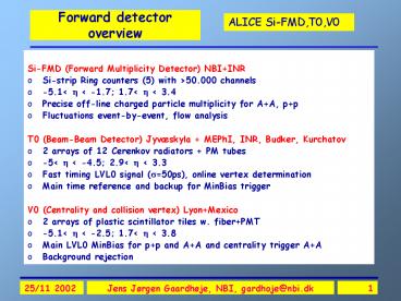
Title: Forward detector overview
1
Forward detector overview
- Si-FMD (Forward Multiplicity Detector) NBIINR
- Si-strip Ring counters (5) with gt50.000 channels
- -5.1lt ? lt -1.7 1.7lt ? lt 3.4
- Precise off-line charged particle multiplicity
for AA, pp - Fluctuations event-by-event, flow analysis
- T0 (Beam-Beam Detector) Jyvæskyla MEPhI, INR,
Budker, Kurchatov - 2 arrays of 12 Cerenkov radiators PM tubes
- -5lt ? lt -4.5 2.9lt ? lt 3.3
- Fast timing LVL0 signal (?50ps), online vertex
determination - Main time reference and backup for MinBias
trigger - V0 (Centrality and collision vertex) LyonMexico
- 2 arrays of plastic scintillator tiles w.
fiberPMT - -5.1lt ? lt -2.5 1.7lt ? lt 3.8
- Main LVL0 MinBias for pp and AA and centrality
trigger AA - Background rejection
2
Forward detectors
V0 1.7 lt h lt 3.8 and 5.1 lt h lt -2.5
Interaction trigger, centrality trigger and
beam-gas rejection. Two arrays of 72 scintillator
tiles readout via fibers
PMD pre-shower det.
T0L
T0R 2.9 lt h lt 3.3 T0 for the
TOF (lt 50 ps time res.) Two arrays of 12 quartz
counters. Also backup to V0
SI-FMD Multiplicity and dn/dh 1.7 lt h lt 3.4
and -5.1 lt h lt -1.7 Silicon pad detector disks
(slow readout)
3
Integration in ALICE
Si-1
V0-R
Si-2
T0-R
Si-3
4
FWD detectors
5
CERN Maquette 11
ITS-pixels
V0-R
T0-R
Si1 (inner)
Si1(outer)
Absorber
6
Si-FMD Overall Geometry
Si1
Si2
Si3
- -5.1lt ? lt-1.7
- 3.4 lt ? lt 1.7
7
Si rings manufactured of 6 wafers
Inner Rin4.2 cm Rout17.2 cm Outer Rin15.4
cm Rout28.4 cm
128
256
10x2x2565120 20x2x1285120
8
Coverage in pseudorapidity
Constraints Vacuum tube outer envelope 42
mm, Outer radius, ITS, Absorber,
cables Background from secondaries(small angles)
Design criteria Largest possible ? coverage
Largest symmetry left and right Overlap between
systems
- Si1
- Out 1.70lt ?lt2.29 In 2.01lt ?lt3.40
- Si2
- Out -2.29lt?lt-1.7 In -3.68lt ?lt-2.28
- Si3
- In -5.09lt ?lt-3.68
- Vertex shift (10cm) d? ? 0.1
?
9
Charged particle occupancy including secondaries
20 ? sectors 256 strips each 5120 channels
20 ? sectors 256 strips each 5120 channels
40 ? sectors 128 strips each 5120 channels
May increase number of strips by factor of 2 or 3
using 128 ch VA-prime PA chip at same cost !
10
Multiplicity resolution
11
Hybrid with Viking PA chips
Connector(s) for power, control, read-out
- Hybrid cards contain
- FEPreampl. chips
- Bias voltages distribution
- Gate/strobe distribution
- Read-out clock distribution
- Detector bias connection
Other components
VA preampshaper 128 ch
Si detector
12
Front end electronics
- REQUIREMENTS
- Adapted for 5-25pF capacitance
- (300?m Si, 0.5 cm2 25pF, 1MIP 22.400 e-)
- Dynamic range 0-20 MIPS
- Radiation hardness gt200kRad
- Peaking time 1-2 ?s
- Low noise (good S/N)
- High integration
- Sample/hold and serial read-out, 10 MHz clock
- Moderate power consumption
- Simple slow controls and power reg.
- Affordable cost
VA1 prime 2 (Viking-IDEAS) Input capacitance lt
30 pF 0-20 MIPs gt1MRad (0.35 ?m tech.) 1-3
?s 475 e- at 25 pF gt S/N 201 128 10 Mhz clock
1.3 mW/ch Test system available OK
13
FMD RO strategy
14
FMD FEE test setup
Labview DAQ
15
Si-FMD timetable (1)
A FRONT END (FE) READ OUT ELECTRONICS Completed
1 Demonstrate functionality of conceptual layout of FEE (Viking PA chip, control system, interface to ALTRO test board) April 1 2003
2 Final choice of VA pre-ampl. chip. RO test June 1, 2003
3 Test FEE system coupled to sample Si detector. Source and electron beam tests. June 1, 2003
4 Design, construction and test of prototype FMD digitizer card (FMDD), RO test with mini FMD-RCU October 1, 2003
5 Full Si detector element electronics chain RO with realistic RCU and DDL link to DAQ. June 1 , 2004
B MECHANICS AND INTEGRATION Completed
1 Full scale model manufactured (Si1) February 1, 2003
2 Cabling and Cooling issues resolved April 1, 2003
3 Full integration sequence decided June 1, 2003
16
Si-FMD timetable (2)
C. SILICON DETECTOR Completed by
1 Complete market survey February 1, 2003
2 Define final specs March 1, 2003
3 Place order for prototype with industry April 1, 2003
4 Delivery Si-wafer prototype June 1, 2003
5 Start production of Si-hybrid FEE card June 1, 2003
6 Delivery prototype hybrid August 1, 2003
7 Si prototype test with FEE and BEE test RO setup December 1, 2003
8 Place final order for Si with industry April1, 2004
17
V0 detector
- Two segmented scintillator hodoscopes on either
side of IP - Minimum bias trigger p-p and Pb-Pb
- Main on-line LVL0 centrality trigger Pb-Pb
- Background filter for the dimuon spectrometer
- Two arm for beam-gas rejection
- Luminosity control
- Multiplicity measurement (high occupancy)
Absorber
V0-R
18
V0 Segmentation
- V0-L and V0-R 5 rings each
- Rings 1-4 30 sectors (12)
- Ring 5 15 sectors (24)
- Rings 1-3 are in the dimuon arm acceptance
Ring V0L V0L V0R V0R
Ring ?max/?min ?max/?min ?max/?min ?max/?min
1 -5.1/-4.6 -0.7/-1.2 3.8/3.4 2.6/3.8
2 -4.6/4.2 -1.2/-1.7 3.4/2.9 3.8/6.3
3 -4.2/-3.7 -1.7/-2.8 2.9/2.5 6.3/9.4
4 -3.7/-3.2 -2.8/-4.7 2.5/2.1 9.4/14.0
5 -3.2/-2.8 -4.7/-7.0 2.1/1.7 14.0/20.7
19
V0 Ligth collection test
- For 1 MIP
- Setup A
- light yield 12 p.e. time resolution (?)
1.6 ns - Setup B
- Light yield 33 p.e. time resolution(?) 1.2
ns
20
V0 Triggering
- LVL 0 triggering with fast electronics (25 ns)
- Dynamic range 1- 300 MIPs
- 1 MIP efficiency gt 97
- Three trigger signals to the CTP corresponding to
3 sum energy levels - LowMB for pp and Pb-Pb (low)
- High central and
- Medium semi-central Pb- Pb
- Simulations AliRoot w/ PYTHIA 6.15 in pp at 7
TeV - L and R single efficiencies 85
- LR 79
- Eff. of Inelastic component 100
- HIJING in Pb-Pb at 5.5 ATeV (to be explored)
21
V0 Timetable
- Ongoing work
- Light optimization ? geometry of the
counter/fiber elements with beam tests -gt end
2002 (OK) - Electronics specification ongoing,
- PM test and choice in Lyon
- Tests of full quadrant w. Beam
- -gt end 2003 (delayed from october
2002)
- Construction in 2004/2005
- V0L by Mexico
- V0R by Lyon
- Electronics by Lyon
- Final system Commissionning
- ? middle 2005
22
T0 Beam-Beam counter
- Precise event timing (?50ps)
- Start detector for ALICE-TOF
- Main LVL0 event trigger
- Pre-trigger for TRD
- Rough on-line vertex determination lt1.5 cm
- Beam-gas suppression
- Output Signals
- T0 (trtl)/2td
- T0v tr-tl
- T0-L, T0-R, Coinc
- Time and energies
- 3 levels of sum energy (low, medium, high)
23
T0 Full scale model
24
T0 elements and beam test
- PM tubes fine mesh
- Hamamatsu R3432-01 (26 mm Ø) or FEU-187 (30 mm Ø)
- 30 mm thick radiator (Lucite)
- Time resolution with broad 1.28GeV/c pion beam
measured to 55ps. - Set threshold at 200 photons
- (1 MIP gives 600 Photons)
Photons in T0-R
Photons in T0-L
25
T0 efficiency
- ALIROOT and Pythia simulations for MB pp
- 200 photon threshold applied
- Coinc. eff (LR) 83
- Left array ?71 and 87
- Right array ?78 and 94
T0-R T0-L
83
T0-R
T0-L
94
87
26
T0 timetable
- RD of Cerenkov detector units
- -HV divider 2 prototypes ready,
- 3rd under const. (OK)
- -Quartz radiators waiting for
- final dimensions (no concern)
- RD of fast electronics unit
- -RD trigger generation unit (CAMAC
- prototype ready)
- -prototype I of CFD (failed, high
- cross-talk but problem solved)
- -prototype II of CFD (ready, very good
- test results)
- -prototype III of CFD (ready, very good
- test results)
- -prototype IV of CFD (DTD) (theo.stud.)
- -time meaner (2 options) (1 prototype ready)
- RD laser calibration system
- Market survey and purchase (manufacturer located
but the purchase is delayed to assure the best
configuration) - Development of the calibration system (still
in study) - RD DAQ and trigger electronics
- Collaboration with TOF to guarantee the required
performance (TOF is only sub-detector requiring
high-precision off-line T0) - Athens has expressed the wish to join. Funding
situation should be clear within a few months. - Mechanical construction
- 11 prototype ready
- TDR progressing as planned
Responsibilities Jyvæskylæ, MEPhI, INR, Budker,
Kurchatov.
27
Summary
- FWD detectors baseline defined
- Physics role defined
- FWD detectors will supply basic day 1 physics
(LVL0 trigger, global reaction information) - Main detector parameters specified
- Concrete prototyping and industrial bids started
- Projects on track
- Aim at TDR by mid-2002
- Main open issues integration and installation
procedures, materials budget (bgd), cooling, Back
End Electronics and DAQ integration, analysis
software
Si-FMD
V0
T0
Recommended
CrystalGraphics Presentations


