
Negative Differential Resistance - PowerPoint PPT Presentation
1 / 29
Title:
Negative Differential Resistance
Description:
DC solution: Vd(Id) IdRL=V. AC solution: V(t)=V v(t); I ... Hysteresis. 1. 2. 3. 485_6. 4. Another case of NDR. V. I. C. B. A. VB. IB. rd=dV/dI; gd=dI/dV. rB 0 ... – PowerPoint PPT presentation
Number of Views:1000
Avg rating:3.0/5.0
Title: Negative Differential Resistance
1
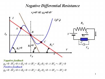
Negative Differential Resistance
rddV/dI gddI/dV
Negative feedback gAgt0 ?VAgt0? ?IAgt0 ? ?VL
?IA?RLgt0 ? ?VA - ?VLlt0 Positive feedback gBlt0
?VBgt0? ?IBlt0 ? ?VL ?IB?RLlt0 ? ?VB - ?VLgt0
2
Stability
DC solution Vd(Id)IdRLV AC solution
V(t)Vv(t) I(t)Ii(t) Vdvd(t)IdRLi(t)RLV
Ii(t)Idid(t)Cdvd/dt Linearize id(t)gd
vd(t) Cdvd/dt gd vd(t)RL-1 vd(t)0
Unstable when gdlt0 gdgtRL-1
3
Switching cycle
I(t)
Hysteresis
V(t)
4
Another case of NDR
rddV/dI gddI/dV
Unstable when rdlt0 rdgtRL
5
Tunnel diode
W
Transition Coefficient
6
I-V characteristics
Tunneling current
Energy conservation
Bias
degenerate doping strength
7
I-V characteristics
8
I-V Characteristics
Assume low temperature
Vgt0
V0
EfpEfn
9
I-V Characteristics
Vgt0
Vgt0
10
I-V Characteristics
VVmax
11
Thyristor
B2
A
G
J1
J2
anode
base1
J3
B1
K
p1
n1
p2
n2
K
A
base2
cathode
1020
1017
1014
12
Reverse Biased State
G
J1
J2
Rev
anode
F
J3
R
n1
p1
p2
n2
A
K
base1
base2
cathode
xn1
Wb1
Reverse Breakover Punch-Through xn1Wb1
Or Avalanche
13
Forward Biased State
Forward Breakover
14
Forward conducting state
G
J1
J2
F
anode
F
J3
F
IK
n1
p1
p2
n2
n1
IA
K
base2
base1
cathode
A
15
I-V Curve
IA
VBF
VBR
IAK
16
Current in the external circuit flows onlywhile
the charge drifts between electrodes
Charge -Q injected at time t1
t1
t2
K
A
Gausss theorem
v
-?0E2SQ2
?0(E2-E1) S-Q
?0E1SQ1
d
-Q
Q1
Q2
Drift region
v
E1
K
A
E2
I(t)
V
x(t)
d
I
V
I(t)
Q1Q2Q
If vconst I(t)Q/(t2-t1)
t1
t2
t
17
IMPATT Diode
IMPact Ionization Avalanche Transit Time Diode
1020
ND-NA
1016
x
1012
ideal
E
real
x
18
IMPATT diode
EAC(T/4)
E(t)
V(t)VDCvAC(t) E(t)EDC EAC(t) EDC?Eb
E(t)
EAC(T/2)0
Eb
TT/4
n(x,t)
x
EAC(3T/4)
E(t)
?TT/4
n(x,t)
Eb
TT/2
x
EAC(T)0
E(t)
Eb
T3T/4
n(x,t)
x
19
IMPATT I-V Characteristics
0 T/2 T 3T/2 2T 5T/2
iAC-vAC rAClt0 PACiACvAC/2lt0 Power is
transferred to the field
Qinj
t
0 T/2 T 3T/2 2T 5T/2
I
iAC
IDC
t
0 T/2 T 3T/2 2T 5T/2
20
Small Signal model
xA
W
p
n
n-
K
A
n
I(t)
rACgt0 ?lt ?A rAClt0 ?gt ?A
Avalanche region
Drift region
rAC
CA?sS/xA
Current in avalanche region is delayed by ?/2
-inductance
Resonance frequency
Typically fvs/2W
21
Power Conversion Efficiency
?max50 in reality 30-35
22
Transferred electron devices
Negative differential mobility ?ddv/dE
v???E vXvs
23
Differential mobility
n?nXnND
24
Instability and domains formation
25
Domain growth
Moving co-ordinate
26
Domain growth
Dielectric relaxation time
Debye length
27
AC operation of Gunn diode
Current is only conductivity current does not
have to be continuous
28
AC operation
Dispersion equation
29
Gunn diode as an amplifier or an oscillator
If ?dlt0 Gexp(?t /?d)gt0 -gain
At the anode
Small gain ?tlt ?d domains are not formed
device is an amplifier Large gain ?tgt ?d
-device is an oscillator
Recommended
CrystalGraphics Presentations


