
Wafer And Integrated Circuits PowerPoint PPT Presentations
All Time
Recommended

United States Wafer And Integrated Circuits IC market competition by top manufacturers/players, with Wafer And Integrated Circuits IC sales volume, price, revenue Million USD and market share for each manufacturer/player; the top players including Entegris, Inc. RTP Company 3M Company ITW ECPS Dalau Brooks Automation, Inc.
| PowerPoint PPT presentation | free to download

This course serves several (CE) goals: replaces part of the ECE ... returns Inductance Trends Inductance vs ... recent studies on dual-material copper ...
| PowerPoint PPT presentation | free to view
integrated circuits * * * * * * * * * * * * * * * * * * * * * * * monolithic diode monolithic resistor monolithic capacitor thin film fabrication vacuum evaporation ...
| PowerPoint PPT presentation | free to download

Integrated Circuits and Manufacturing 1-24-2003
| PowerPoint PPT presentation | free to download
Avogadro-Scale Engineering: Form and Function. MIT, November 18, ... Crystallization of -Si. Bulk Si. n /p n /p n /p Gate. Gate. T1. T2. M1. M2. M3. M4. n /p ...
| PowerPoint PPT presentation | free to download

Digital Integrated Circuits Design NTUEE Course by Prof. An-Yeu Wu Introduction July 30, 2002 What is this Course all about? Introduction to digital integrated circuits.
| PowerPoint PPT presentation | free to download

... stategy meetings, presentations, quizzes. CS252/Patterson. Lec 2.8 ... funny times, as most systems can't access all of 2nd level cache without TLB misses! ...
| PowerPoint PPT presentation | free to view

Are you looking for wafer robot repair solutions? Kensington Laboratories offers certified products of precision handling robots to stage repair programs that can help smooth out industry operations and offer you value for money.
| PowerPoint PPT presentation | free to download

Energy is supplied by an RF generator, causing a gas plasma between the ... a random number was generated for each, and then the random numbers were ordered. ...
| PowerPoint PPT presentation | free to view
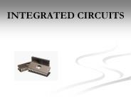
Integrated circuit (IC), also called microelectronic circuit or chip and it is a small electrical circuit created using a semiconductor substance, such as silicon. IC chips are found in nearly every modern electronic devices.
| PowerPoint PPT presentation | free to download

Using refractory metals and silicides can reduce the sheet resistance of gate ... One approach is to use a refractory metal silicide on top of the polysilicon ...
| PowerPoint PPT presentation | free to view

Propagation delay, noise margins, and power dissipation. Sequential circuits. ... Power delivery and dissipation will be prohibitive. Courtesy, Intel. EE141. 19 ...
| PowerPoint PPT presentation | free to view

The general Characteristics of both Thin-film and Thick-film IC's are similar to ... Circuits use Evaporation or Cathode-sputtering techniques in forming the passive ...
| PowerPoint PPT presentation | free to view

... 950 to 1150 oC & at the same time, exposed to a gas containing O2 or H2O or both. ... HIGH FREQUENCY MODEL OF OPAMP. 32. AC characteristics. Frequency Response ...
| PowerPoint PPT presentation | free to view
Electrical characterization, metallurgical investigation, and thermal stability ... Gain.under large-signal conditions ...gain is less than MAG/MSG... Breakdown ...
| PowerPoint PPT presentation | free to download

The First Integrated Circuits. Bipolar logic. 1960's. ECL 3 ... E = Energy per operation = Pav tp. Energy-Delay Product (EDP) = quality metric of gate = E tp ...
| PowerPoint PPT presentation | free to view

... P P P P P P P P P P P P P P P P P P P P P P P P PPP P P P P P P P P ... 456789:CDEFGHIJSTUVWXYZcdefghijstuvwxyz GpSs tFTO ...
| PowerPoint PPT presentation | free to view

The semiconductor industry is improving daily, either for the production equipment manufacturers or the end-users. In fact, the transistors in the integrated circuit are getting increased along with the performance.
| PowerPoint PPT presentation | free to download
by thinning the collector while increasing current. Challenges with Scaling ... Compromise: physically undercut the collector semiconductor. Emitter Ohmic Resistivity: ...
| PowerPoint PPT presentation | free to download

Characterization, Modeling and Optimization of Fills and Stress in Semiconductor Integrated Circuits
| PowerPoint PPT presentation | free to download

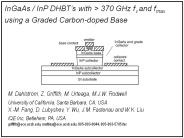
for Optical Fiber and ... HBT S12 is very small Standard 12-term VNA calibrations ... For a BPSK point-point digital microwave radio link. Ptransmitter. transmission.
| PowerPoint PPT presentation | free to download

'Lithography limits for Nanophotonic devices' JRA2 : EPFL-IPEQ ' ... (e-beam lithography and dry etching) Technology Integration Platforms. 25 ...
| PowerPoint PPT presentation | free to view

Wafer level packaging (WLP) is a method of attaching packaging components to an integrated circuit (IC) prior to dicing the wafer. This procedure varies from a traditional method, which involve slicing the wafer into separate circuits (dice) before attaching the packaging components.
| PowerPoint PPT presentation | free to download

An Integrated Circuit is generally expressed in the form of a chip. Made in one unit, it’s an electrical parts assembly. However, a wafer represents small slices of silicon. In the production of integrated circuits like the integrated circuits are used in most semiconductor wafers, these are utilized.
| PowerPoint PPT presentation | free to download

The semiconductor industry is undergoing rapid growth, and silicon wafer manufacturing companies are key to this success. A silicon wafer is a thin piece of semiconductor material used in the fabrication of integrated circuits.
| PowerPoint PPT presentation | free to view

Silicon Carbide Wafers are the foundation for LED components. Integrated Circuits, ICs, which are found in all digital devices, are made from silicon wafer manufacturers.
| PowerPoint PPT presentation | free to view

Wafer market by Size (150 mm, 200mm, 300mm, and 450mm), by Type (N-type and P-type), by Application (Solar cells, Integrated Circuits, Photoelectric Cells, and Others) - Forecast 2016-2022
| PowerPoint PPT presentation | free to download

Wafer-level packaging (WLP) is the technology of packaging an integrated circuit while still part of the wafer, in contrast to the more conventional method of slicing the wafer into individual circuits (dice) and then packaging them. Wafer-Level Packaging includes Fan-in WLP and Fan-out WLP on the base of classification.
| PowerPoint PPT presentation | free to download
Silicon Wafers industry by Size (150 mm, 200mm, 300mm, and 450mm), by Type (N-type and P-type), by Application (Solar cells, Integrated Circuits, Photoelectric Cells, and Others) - Forecast 2016-2022
| PowerPoint PPT presentation | free to download

In the fast-paced semiconductor manufacturing industry, optimizing yield and maintaining high-quality standards are paramount. As integrated circuits continue to shrink in size and increase in complexity, the necessity for precise, advanced methodologies becomes ever more critical. Among the technologies employed, wafer map software stands out as an indispensable tool. Leveraging complex algorithms, color-coded grids, and innovative software functionalities, advanced wafer mapping enables real-time analysis of semiconductor wafers at an unparalleled level of detail. This technology has dramatically transformed the industry, providing insights into defect patterns, yield calculations, and testing processes, hence enhancing semiconductor manufacturing efficiency and productivity. This blog delves into the intricacies of wafer mapping, exploring its role, advancements, and impact on semiconductor manufacturing.
| PowerPoint PPT presentation | free to download

Epitaxial wafers are a key component in the semiconductor industry. They are used to produce high-quality, single-crystal layers of semiconductor materials on a substrate, which are then used in the manufacturing of various electronic devices. These wafers are essential for the production of advanced semiconductors, such as integrated circuits, power devices, and sensors. The demand for epitaxial wafers is driven by the growing need for advanced and efficient electronic devices across various industries.
| PowerPoint PPT presentation | free to download

These semiconductors are used in the creation of ICs due to the peculiarity of electrical currents via sic wafer CA (integrated circuits). In many electrical gadgets, the ICs serve as orders for certain tasks.
| PowerPoint PPT presentation | free to view

Wafer reclaim is a silicon wafer which has been polished, cleaned and processed so that they can be used for the different applications such as solar cells, integrated circuits and others. The costs of this reclaimed wafer are very less and the quality is very good as well. These silicon wafers are thin in size and caters same features as the virgin test wafers. They are mainly used in integrated circuits and many companies also use these silicon wafers for their product testing.
| PowerPoint PPT presentation | free to download

Global Silicon Wafer Reclaim Market Research Report: By Wafer Diameter (150 MM, 200 MM, 300 MM and others), by Application (Integrated Circuits, Solar Cells, Photoelectric Cells and others), by Region (North America, Europe, Asia-Pacific and Rest of the World) - Forecast till 2025. Silicon wafer reclaim is a multi-step process that transforms a used wafer with multiple layers of various materials into a qualification wafer. The major steps included in wafer reclaim are sorting. stripping, lapping and grinding, polishing, cleaning, and inspection. Browse Complete Report Details: https://www.marketresearchfuture.com/reports/silicon-wafer-reclaim-market-8246
| PowerPoint PPT presentation | free to download

With the rapid expansion in the electronics industry, there has been increasing demand for microelectromechanical systems (MEMS), microchips and integrated circuits for manufacturing various consumer electronic goods, including smartphones, laptops and desktops Get a PDF Sample for more detailed market insights: Visit the following link: https://www.imarcgroup.com/semiconductor-wafer-polishing-grinding-equipment-market E-mail: sales@imarcgroup.com Contact: +91-120-415-5099
| PowerPoint PPT presentation | free to download

Download Free Research Report PDF : http://bit.ly/2MHjlHc A Semiconductor glass wafer is usually a very thin disc used as a base for manufacturing integrated circuits. It is a thin piece of semiconductor material, usually made of borosilicate glass, quartz, or fused silica.
| PowerPoint PPT presentation | free to download

Wafer backgrinding is a semiconductor device fabrication step during which wafer thickness is reduced to allow stacking and high-density packaging of integrated circuits (IC). In the context of China-US trade war and global economic volatility and uncertainty, it will have a big influence on this market. Wafer Backgrinding Tape Report by Material, Application, and Geography ? Global Forecast to 2023 is a professional and comprehensive research report on the world?s major regional market conditions, focusing on the main regions (North America, Europe and Asia-Pacific) and the main countries (United States, Germany, United Kingdom, Japan, South Korea and China).
| PowerPoint PPT presentation | free to download

Gallium Arsenide (GaAs) Market Size is forecast to reach $2.2 billion by 2027, growing at a CAGR of 11.1% during 2022-2027. GaAs is increasingly used as a replacement for silicon because of its enhanced electronic properties and was selectively grown on GaAs substrates patterned with SiO2 by conventional molecular beam semiconductor device epitaxy. Moreover growing demand for GaAs solutions such as laser diodes, light emitting diodes, optoelectronic devices and Monolithic Microwave Integrated Circuits across various end-user industries such as aerospace & defense, electronics, and communications is analyzed to drive the GaAs Wafer Market share.
| PowerPoint PPT presentation | free to download

A glass wafer is usually a very thin disc used as a base for manufacturing integrated circuits. It is a thin piece of semiconductor material, usually made of borosilicate glass, quartz, or fused silica.In terms of geographic regions, APAC will contribute to major semiconductor glass wafer market growth. This is due to the strong presence of electronics manufacturers. Moreover, the presence of several foundries in countries such as China, Japan, South Korea, and Taiwan will also significantly contribute to the growth of the market in APAC.
| PowerPoint PPT presentation | free to download

Lithography equipment is widely used and designed for printing complex circuit designs on silicon wafers which are mostly raw materials for integrated circuits (ICs).
| PowerPoint PPT presentation | free to download

Advanced packaging is specially designed to improve the device performance by using integrated circuits which protect the metallic part from damaging. 3D integrated circuits, 2.5D integrated circuits, fan out wafer level package and among others are some of the common types of advanced packaging technologies. Different types of integrated circuits are manufactured as per the need of the packaging. They are widely used in industries such as healthcare, automotive, aerospace, defense and others.
| PowerPoint PPT presentation | free to download
Thin wafer, which are the thin slices of semiconductor, are largely being used for manufacturing integrated circuits (ICs). They are extensively used across automotive sector owing to the elevating demand for AI-chipsets that are developed using thin wafer technology. Get sample copy of this research report @ https://www.gminsights.com/request-sample/detail/5007
| PowerPoint PPT presentation | free to download

MCM: multi-chip modules: high speed and density. 13. Summary. Electronics aspects of digital design. Integrated Circuits (wafer, die, SSI, MSI, LSI, VLSI) ...
| PowerPoint PPT presentation | free to view

Semiconductor manufacturing is an intricate process involving numerous stages, from wafer preparation to the final packaging of the integrated circuit.
| PowerPoint PPT presentation | free to download

Wafer Fabrication CZ processing Float Zone Processing Typical defects in crystals Photolithography Typical Photoresist Problems Example Estimate the resolution and ...
| PowerPoint PPT presentation | free to view

Silicon wafer reclaim is a type of multi-step procedure which transforms a used wafer with numerous layers of various materials into a qualification wafer. The major steps integrated in wafer reclaim are sorting, stripping, lapping and grinding, polishing, cleaning and the inspection.
| PowerPoint PPT presentation | free to download

Indium Phosphide Wafer Market Size is forecast to reach $82.8 million by 2026, at a CAGR of 8.12% during 2021-2026. The indium phosphide wafers offers a superior electron velocity as compared to other popular semiconductors such as silicon.
| PowerPoint PPT presentation | free to download

Silicon on insulator is a fabrication technique that mainly uses pure form of crystal silicon and silicon oxide for microchips and integrated circuits. This technology also uses layered silicon–insulator–silicon substrate in place of conventional silicon substrates which are applicable for manufacturing of semiconductors. This technology is having many applications in SOI wafers, high performance radio frequency, microelectronics and photonics.
| PowerPoint PPT presentation | free to download

Indium Phosphide Wafer Market Size is forecast to reach $82.8 million by 2026, at a CAGR of 8.12% during 2021-2026.
| PowerPoint PPT presentation | free to download

Indium Phosphide Wafer Market Size is forecast to reach $82.8 million by 2026, at a CAGR of 8.12% during 2021-2026.
| PowerPoint PPT presentation | free to download

Silicon wafers exist in a wide range of sizes, and various varieties of diameters. The variety of sizes allows the tech industry to have the freedom to use a specifically sized wafer in various gadgets.
| PowerPoint PPT presentation | free to view

Wafer Cleaning equipment market report categorizes the global market based on types, equipment, and applications forecasting revenue of wafer cleaning equipment market from 2012 to 2017.
| PowerPoint PPT presentation | free to download
Semiconductor Silicon Wafer Market By Process (BEOL, FEOL), by Application (Consumer Electronics, IT, Healthcare, BFSI, Telecom, Automotive) - Forecast 2022
| PowerPoint PPT presentation | free to download

semiconductor wafer market share By Process (BEOL, FEOL), by Application (Consumer Electronics, IT, Healthcare, BFSI, Telecom, Automotive)- Forecast 2016-2022
| PowerPoint PPT presentation | free to download
semiconductor wafer fabrication market By Process (BEOL, FEOL), by Application (Consumer Electronics, IT, Healthcare, BFSI, Telecom, Automotive)- Forecast 2016-2022
| PowerPoint PPT presentation | free to download
semiconductor wafer market size By Process (BEOL, FEOL), by Application (Consumer Electronics, IT, Healthcare, BFSI, Telecom, Automotive)- Forecast 2016-2022
| PowerPoint PPT presentation | free to download